|
|
|
PDF AS29LV400 Data sheet ( Hoja de datos )
| Número de pieza | AS29LV400 | |
| Descripción | 3V 512K x 8 / 256K x 16 CMOS Flash EEPROM | |
| Fabricantes | Alliance Semiconductor | |
| Logotipo | ||
Hay una vista previa y un enlace de descarga de AS29LV400 (archivo pdf) en la parte inferior de esta página. Total 25 Páginas | ||
|
No Preview Available !
Preliminary Information
March 2001
AS29LV400
®
3V 512K x 8/256K × 16 CMOS Flash EEPROM
Features
• Organization: 512Kx8/256Kx16
• Sector architecture
- One 16K; two 8K; one 32K; and seven 64K byte sectors
- One 8K; two 4K; one 16K; and seven 32K word sectors
- Boot code sector architecture—T (top) or B (bottom)
- Erase any combination of sectors or full chip
• Single 2.7-3.6V power supply for read/write operations
• Sector protection
• High speed 70/80/90/120 ns address access time
• Automated on-chip programming algorithm
- Automatically programs/verifies data at specified address
• Automated on-chip erase algorithm
- Automatically preprograms/erases chip or specified
sectors
• Hardware RES ET pin
- Resets internal state machine to read mode
• Low power consumption
- 200 nA typical automatic sleep mode current
- 200 nA typical standby current
- 10 mA typical read current
• JEDEC standard software, packages and pinouts
- 48-pin TSOP
- 44-pin SO; availabillity TBD
• Detection of program/erase cycle completion
- DQ7 DATA polling
- DQ6 toggle bit
- DQ2 toggle bit
- RY/B Y output
• Erase suspend/resume
- Supports reading data from or programming data to a
sector not being erased
• Low VCC write lock-out below 1.5V
• 10 year data retention at 150C
• 100,000 write/erase cycle endurance
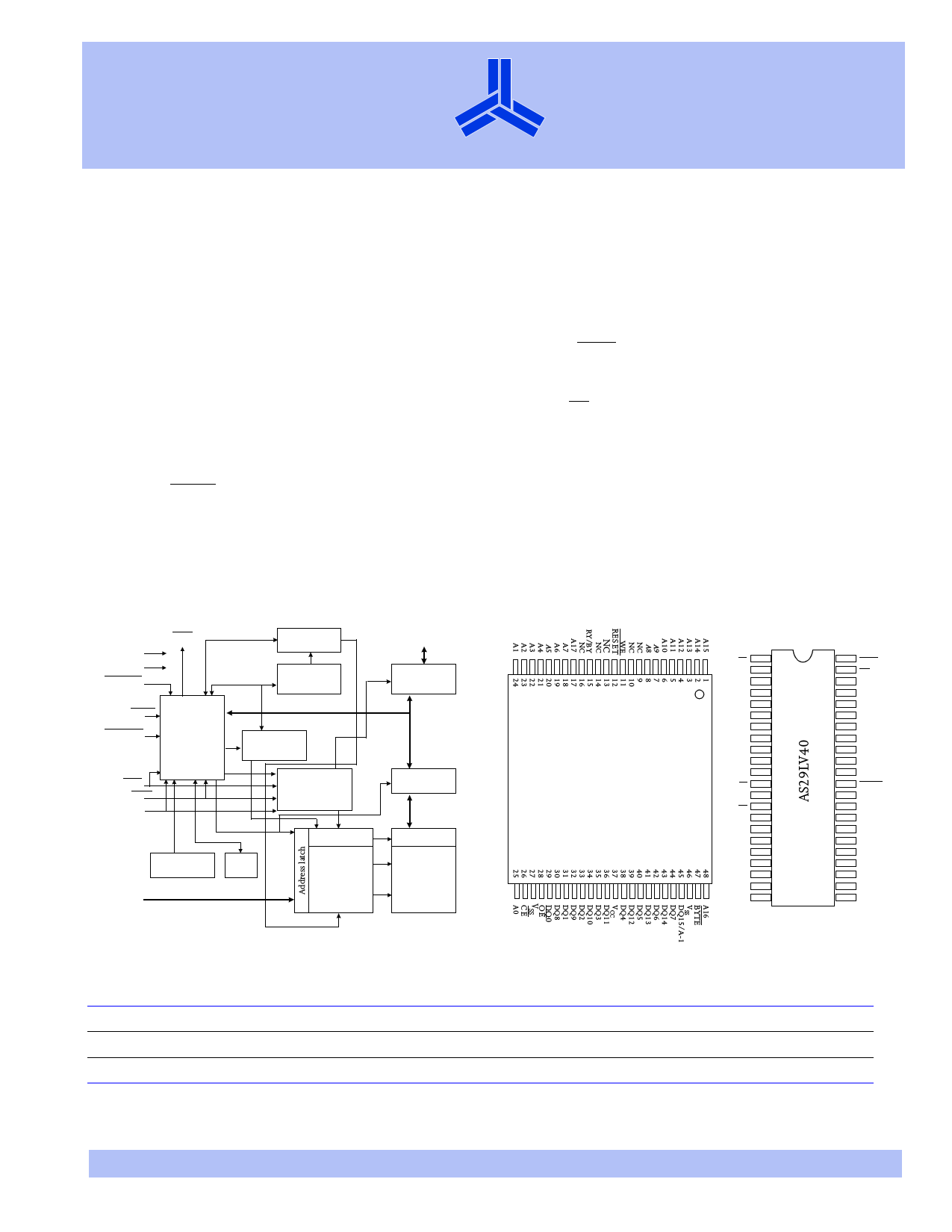
Logic block diagram
VCC
VSS
RESET
RY/B Y
Sector protect/
erase voltage
switches
Erase voltage
generator
DQ0–DQ15
Input/output
buffers
WE
BYTE
Program/erase
control
Command
register
CE
OE
A-1
Program voltage
generator
Chip enable
Output enable
Logic
STB Data latch
STB Y decoder
Y gating
VCC detector
Timer
A0–A17
X decoder
Cell matrix
Pin arrangement
48-pin TSOP
AS29LV40
44-pin SO
RY/BY
NC
A17
A7
A6
A5
A4
A3
A2
A1
A0
CE
VSS
OE
DQ0
DQ8
DQ1
DQ9
DQ2
DQ10
DQ3
DQ11
1
2
3
4
5
6
7
8
9
10
11
12
13
14
15
16
17
18
19
20
21
22
44 RESET
43 WE
42 A8
41 A9
40 A10
39 A11
38 A12
37 A13
36 A14
35 A15
34 A16
33 BY TE
32 VSS
31 DQ15/A-1
30 DQ7
29 DQ14
28 DQ6
27 DQ13
26 DQ5
25 DQ12
24 DQ4
23 VCC
Selection guide
Maximum access time
Maximum chip enable access time
Maximum output enable access time
29LV400-70 29LV400-80 29LV400-90 29LV400-120
tAA 70 80 90 120
tCE 70 80 90 120
tOE 30
30
35
50
Unit
ns
ns
ns
3/20/01; V.0.9.3
Alliance Semiconductor
P. 1 of 25
Copyright © Alliance Semiconductor. All rights reserved.
1 page 
March 2001
ID Sector address table
Bottom boot sector address
(AS29LV400B)
Sector A17 A16 A15 A14 A13 A12
0 00000X
1 000010
2 000011
3 0001XX
4 001XXX
5 010XXX
6 011XXX
7 100XXX
8 101XXX
9 110XXX
10 1 1 1 X X X
AS29LV400
®
Top boot sector address
(AS29LV400T)
A17 A16 A15 A14 A13 A12
0 0 0 XXX
0 0 1 XXX
0 1 0 XXX
0 1 1 XXX
1 0 0 XXX
1 0 1 XXX
1 1 0 XXX
1110XX
111100
111101
11111X
READ codes
Mode
MFR code (Alliance Semiconductor)
Device code
×8 T boot
×8 B boot
×16 T boot
×16 B boot
Sector protection
Key: L =Low (<VIL); H = High (>VIH); X =Don’t care
A17–A12
A6 A1 A0 Code
X L L L 52h
X L L H B9h
X L L H BAh
X L L H 22B9h
X L L H 22BAh
Sector address L
HL
01h protected
00h unprotected
3/20/01; V.0.9.3
Alliance Semiconductor
P. 5 of 25
5 Page 
March 2001
Automated on-chip programming algorithm
START
Write program command sequence
(see below)
DATA polling or toggle bit
successfully completed
Increment
address
Last
address?
NO
YES
Programming completed
AS29LV400
®
Automated on-chip erase algorithm
START
Write erase command sequence
(see below)
DATA polling or toggle bit
successfully completed
Erase complete
Chip erase command sequence
×16 mode (address/data):
555h/AAh
Individual sector/multiple sector
erase command sequence
×16 mode (address/data):
555h/AAh
2AAh/55h
2AAh/55h
555h/80h
555h/80h
Program command sequence
×16 mode (address/data):
555h/AAh
2AAh/55h
555h/A0h
Program address/program data
555h/AAh
2AAh/55h
555h/10h
555h/AAh
2AAh/55h
Sector address/30h
Sector address/30h
Sector address/30h
3/20/01; V.0.9.3
optional sector erase commands
† The system software should check the status of DQ3 prior to and following each
subsequent sector erase command to ensure command completion. The device may
not have accepted the command if DQ3 is high on second status check.
Alliance Semiconductor
P. 11 of 25
11 Page | ||
| Páginas | Total 25 Páginas | |
| PDF Descargar | [ Datasheet AS29LV400.PDF ] | |
Hoja de datos destacado
| Número de pieza | Descripción | Fabricantes |
| AS29LV400 | 3V 512K x 8 / 256K x 16 CMOS Flash EEPROM | Alliance Semiconductor |
| Número de pieza | Descripción | Fabricantes |
| SLA6805M | High Voltage 3 phase Motor Driver IC. |
Sanken |
| SDC1742 | 12- and 14-Bit Hybrid Synchro / Resolver-to-Digital Converters. |
Analog Devices |
|
DataSheet.es es una pagina web que funciona como un repositorio de manuales o hoja de datos de muchos de los productos más populares, |
| DataSheet.es | 2020 | Privacy Policy | Contacto | Buscar |