|
|
|
PDF NCV4264-2 Data sheet ( Hoja de datos )
| Número de pieza | NCV4264-2 | |
| Descripción | Low Dropout Linear Regulator | |
| Fabricantes | ON Semiconductor | |
| Logotipo | ||
Hay una vista previa y un enlace de descarga de NCV4264-2 (archivo pdf) en la parte inferior de esta página. Total 11 Páginas | ||
|
No Preview Available !
NCV4264-2
Low IQ Low Dropout
Linear Regulator
The NCV4264−2 is functionally and pin for pin compatible with
NCV4264 with a lower quiescent current consumption. Its output
stage supplies 100 mA with "2.0% output voltage accuracy.
Maximum dropout voltage is 500 mV at 100 mA load current.
It is internally protected against 45 V input transients, input supply
reversal, output overcurrent faults, and excess die temperature. No
external components are required to enable these features.
Features
• 3.3 V and 5.0 V Fixed Output
• "2.0% Output Accuracy, Over Full Temperature Range
• 60 mA Maximum Quiescent Current at IOUT = 100 mA
• 500 mV Maximum Dropout Voltage at 100 mA Load Current
• Wide Input Voltage Operating Range of 4.5 V to 45 V
• AEC−Q100 Grade 1 Qualified and PPAP Capable
• Internal Fault Protection
♦ −42 V Reverse Voltage
♦ Short Circuit/Overcurrent
♦ Thermal Overload
• This is a Pb−Free Device
http://onsemi.com
MARKING
DIAGRAM
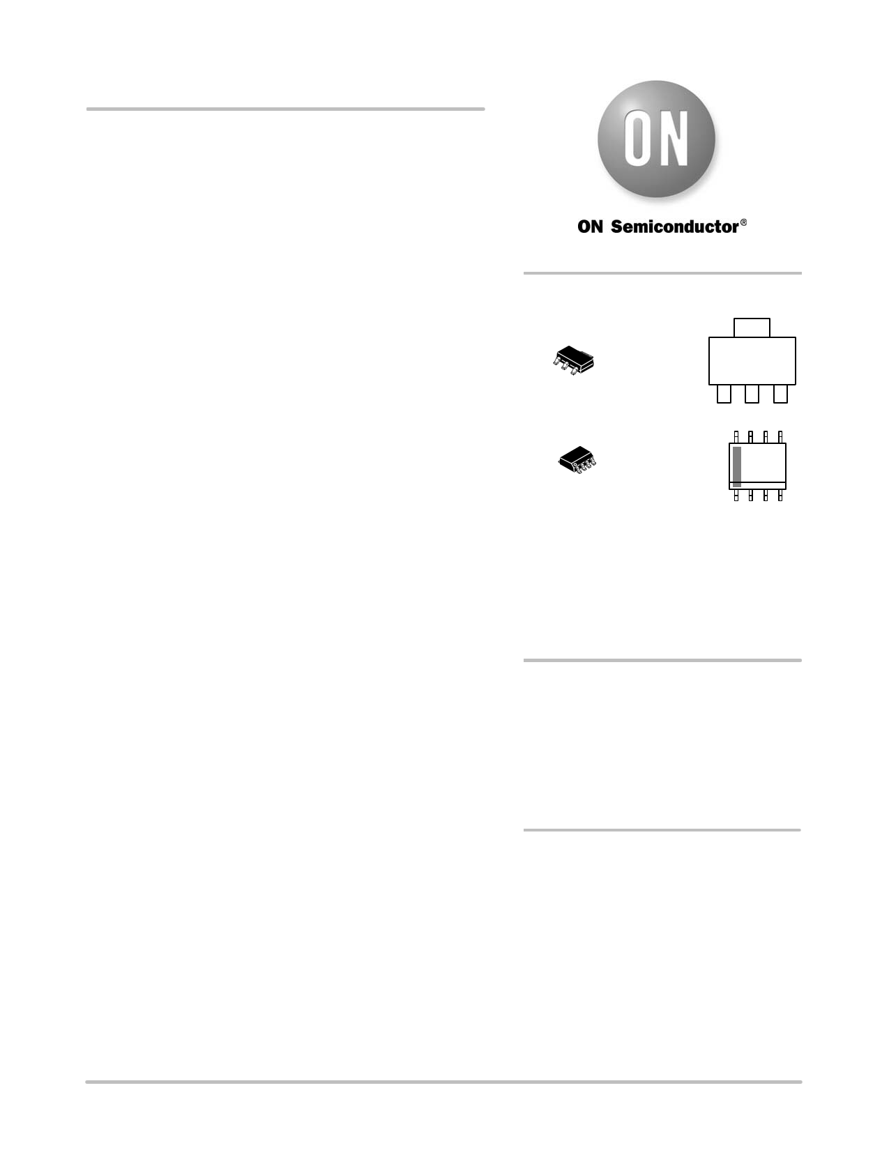
TAB
12 3
SOT−223
ST SUFFIX
CASE 318E
AYW
V642xG
G
1
8
1
SOIC−8 Fused
CASE 751
8
V642x
ALYWX
G
1
x = 5 (5.0 V Version)
= 3 (3.3 V Version)
A = Assembly Location
L = Wafer Lot
Y = Year
W = Work Week
G = Pb−Free Package
(Note: Microdot may be in either location)
PIN CONNECTIONS
(SOT−223)
PIN FUNCTION
1 VIN
2,TAB GND
3 VOUT
(SOIC−8 Fused)
PIN FUNCTION
1 NC
2, VIN
3 GND
4.
5−8.
VOUT
NC
ORDERING INFORMATION
See detailed ordering and shipping information in the package
dimensions section on page 9 of this data sheet.
© Semiconductor Components Industries, LLC, 2014
November, 2014 − Rev. 8
1
Publication Order Number:
NCV4264−2/D
1 page 
NCV4264−2
TYPICAL CHARACTERISTIC CURVES − 5 V Version
180
160
140
120
100
80
TA = 25°C
60
40
20
0
0
TA = 125°C
10 20 30 40 50
INPUT VOLTAGE (V)
Figure 8. Output Current vs. Input Voltage
(5 V Version)
6.0
5.0
4.0
3.0
2.0
1.0
0
0
RL = 50 W
2.0 4.0 6.0
INPUT VOLTAGE (V)
8.0
Figure 9. Input Voltage vs. Output Voltage
(5 V Version)
10
16
14
12
10
8
6
RL = 50 W
4
2
0 RL = 100 W
0 10 20 30 40 50
INPUT VOLTAGE (V)
Figure 10. Quiescent Current vs. Input Voltage
(5 V Version)
http://onsemi.com
5
5 Page 
NCV4264−2
PACKAGE DIMENSIONS
−X−
A
SOIC−8 NB
CASE 751−07
ISSUE AK
B
−Y−
−Z−
H
85
S 0.25 (0.010) M Y M
1
4
K
G
D
C
SEATING
PLANE
N X 45_
0.10 (0.004)
M
J
0.25 (0.010) M Z Y S X S
SOLDERING FOOTPRINT*
NOTES:
1. DIMENSIONING AND TOLERANCING PER
ANSI Y14.5M, 1982.
2. CONTROLLING DIMENSION: MILLIMETER.
3. DIMENSION A AND B DO NOT INCLUDE
MOLD PROTRUSION.
4. MAXIMUM MOLD PROTRUSION 0.15 (0.006)
PER SIDE.
5. DIMENSION D DOES NOT INCLUDE DAMBAR
PROTRUSION. ALLOWABLE DAMBAR
PROTRUSION SHALL BE 0.127 (0.005) TOTAL
IN EXCESS OF THE D DIMENSION AT
MAXIMUM MATERIAL CONDITION.
6. 751−01 THRU 751−06 ARE OBSOLETE. NEW
STANDARD IS 751−07.
MILLIMETERS
INCHES
DIM MIN MAX MIN MAX
A 4.80 5.00 0.189 0.197
B 3.80 4.00 0.150 0.157
C 1.35 1.75 0.053 0.069
D 0.33 0.51 0.013 0.020
G 1.27 BSC 0.050 BSC
H 0.10 0.25 0.004 0.010
J 0.19 0.25 0.007 0.010
K 0.40 1.27 0.016 0.050
M 0_ 8_ 0_ 8_
N 0.25 0.50 0.010 0.020
S 5.80 6.20 0.228 0.244
1.52
0.060
7.0
0.275
4.0
0.155
0.6
0.024
1.270
0.050
ǒ ǓSCALE 6:1
mm
inches
*For additional information on our Pb−Free strategy and soldering
details, please download the ON Semiconductor Soldering and
Mounting Techniques Reference Manual, SOLDERRM/D.
ON Semiconductor and
are registered trademarks of Semiconductor Components Industries, LLC (SCILLC). SCILLC owns the rights to a number of patents, trademarks,
copyrights, trade secrets, and other intellectual property. A listing of SCILLC’s product/patent coverage may be accessed at www.onsemi.com/site/pdf/Patent− Marking.pdf. SCILLC
reserves the right to make changes without further notice to any products herein. SCILLC makes no warranty, representation or guarantee regarding the suitability of its products
for any particular purpose, nor does SCILLC assume any liability arising out of the application or use of any product or circuit, and specifically disclaims any and all liability, including
without limitation special, consequential or incidental damages. “Typical” parameters which may be provided in SCILLC data sheets and/or specifications can and do vary in different
applications and actual performance may vary over time. All operating parameters, including “Typicals” must be validated for each customer application by customer’s technical
experts. SCILLC does not convey any license under its patent rights nor the rights of others. SCILLC products are not designed, intended, or authorized for use as components
in systems intended for surgical implant into the body, or other applications intended to support or sustain life, or for any other application in which the failure of the SCILLC product
could create a situation where personal injury or death may occur. Should Buyer purchase or use SCILLC products for any such unintended or unauthorized application, Buyer shall
indemnify and hold SCILLC and its officers, employees, subsidiaries, affiliates, and distributors harmless against all claims, costs, damages, and expenses, and reasonable attorney
fees arising out of, directly or indirectly, any claim of personal injury or death associated with such unintended or unauthorized use, even if such claim alleges that SCILLC was
negligent regarding the design or manufacture of the part. SCILLC is an Equal Opportunity/Affirmative Action Employer. This literature is subject to all applicable copyright laws
and is not for resale in any manner.
PUBLICATION ORDERING INFORMATION
LITERATURE FULFILLMENT:
Literature Distribution Center for ON Semiconductor
P.O. Box 5163, Denver, Colorado 80217 USA
Phone: 303−675−2175 or 800−344−3860 Toll Free USA/Canada
Fax: 303−675−2176 or 800−344−3867 Toll Free USA/Canada
Email: [email protected]
N. American Technical Support: 800−282−9855 Toll Free
USA/Canada
Europe, Middle East and Africa Technical Support:
Phone: 421 33 790 2910
Japan Customer Focus Center
Phone: 81−3−5817−1050
ON Semiconductor Website: www.onsemi.com
Order Literature: http://www.onsemi.com/orderlit
For additional information, please contact your local
Sales Representative
http://onsemi.com
11
NCV4264−2/D
11 Page | ||
| Páginas | Total 11 Páginas | |
| PDF Descargar | [ Datasheet NCV4264-2.PDF ] | |
Hoja de datos destacado
| Número de pieza | Descripción | Fabricantes |
| NCV4264-2 | Low Dropout Linear Regulator | ON Semiconductor |
| NCV4264-2C | Low Dropout Linear Regulator | ON Semiconductor |
| Número de pieza | Descripción | Fabricantes |
| SLA6805M | High Voltage 3 phase Motor Driver IC. |
Sanken |
| SDC1742 | 12- and 14-Bit Hybrid Synchro / Resolver-to-Digital Converters. |
Analog Devices |
|
DataSheet.es es una pagina web que funciona como un repositorio de manuales o hoja de datos de muchos de los productos más populares, |
| DataSheet.es | 2020 | Privacy Policy | Contacto | Buscar |