|
|
|
PDF GP1R Data sheet ( Hoja de datos )
| Número de pieza | GP1R | |
| Descripción | Dual Mode CDMA/AMPS Baseband Interface | |
| Fabricantes | Mitel Networks Corporation | |
| Logotipo | ||
Hay una vista previa y un enlace de descarga de GP1R (archivo pdf) en la parte inferior de esta página. Total 15 Páginas | ||
|
No Preview Available !
PLUTO
Dual Mode CDMA/AMPS Baseband Interface
Advance Information
DS4722 - 1.8 July 1998
The PLUTO baseband interface circuit is designed for use
in dual mode CDMA/AMPS digital cellular telephones. In the
telephone, Pluto provides the interface between the radio (RF
& IF) components and the baseband digital signal processor.
Pluto is part of a complete chipset solution for CDMA phones
entitled the Planet chipset.
The receive (RX) section converts the analog in-phase and
quadrature (I & Q) signals into equivalent digital signals whilst
the transmit (TX) circuits perform the complementary function
of translating digital baseband information into the analog
equivalent signals required for the modulator in the radio
circuits. VHF PLLS are also included for second RXLO and
TXIF generation.
PLUTO also contains a 4 channel general purpose ADC
which is included for such purposes as environmental and
signal strength monitoring.
FEATURES
s Dual mode AMPS/CDMA compatible
s Low Power/Low Voltage operation
s Standard baseband I and Q interface
s 4 Input Auxiliary ADC
s Synthesisers
APPLICATIONS
s Dual Mode CDMA/AMPs digital cellular
telephones
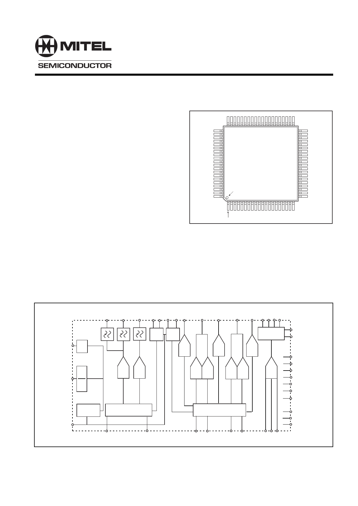
PIN 80
PIN 1 IDENT
PIN 1 GMPP8028
Figure 1 Pin connections - top view
ABSOLUTE MAXIMUM RATINGS
Supply voltage
Voltage applied to any other pin
Operating junction temperature
Storage temperature
ESD (human body model)
-0.3 to 3.9V
-0.3 to Vcc+0.3V
150°C
-55°C to 150°C
2kV
ORDERING INFORMATION
PLUTO/KG/GP1R
TXQ,TXQ-
TXIF PD_RX
FM_MOD
TXI,TXI- PD_TX RXIF
FC_I
I+,I-
BAL
Q+,Q-
ADC<3> ADC<1>
FC_Q ADC<2> ADC<0>
TCXO/4
/4
CHIPx8
1025
512
19.68MHz
BUFFER
TCXO
TX RX
SYNTH SYNTH
8-BIT
DAC
8-BIT
DAC
ANALOG
MULTIPLEXER
8-BIT
DAC
8-BIT
DAC
8-BIT
DAC
8-BIT 6-BIT
ADC ADC
6-BIT 8-BIT
ADC ADC
8-BIT
ADC
S<0>
S<1>
VDD
GND
SUB
FM/
SLEEP/
IDLE/
RESET/
tx calibration and control
rx calibration and control
SDATA
SCLOCK
SLATCH
TXCLK
TXD<7:0>
RXIFMDATA
RXID<3:0>
ADCENA ADCDATA
RXQFMDATA
RXQD<3:0>
ADCCLK
Figure 2 Block diagram
1 page 
PLUTO
TIMING INFORMATION
Parameter
t1 TXCLOCK PERIOD (CDMA TX)
t2 TXCLOCK HIGH TIME (CDMA TX)
t3 TXCLOCK LOW TIME (CDMA TX)
t4 TXCLOCK PHASE Delay (CDMA TX)
t5 TXCLOCK RISE TIME (CDMA TX)
t6 TXCLOCK FALL TIME (CDMA TX)
t7 TXD-TXCLOCK SETUP TIME
t8 TXCLOCK-TXD HOLD TIME
t11 TXCLOCK PERIOD (FM TX)
t12 TXCLOCK HIGH TIME (FM TX)
t13 TXCLOCK LOW TIME (FM TX)
t14 CHIPx8 PERIOD
t15 CHIPx8 HIGH TIME
t16 CHIPx8LOW TIME
t17 CHIPx8 RISE TIME
t18 CHIPx8 FALL TIME
t19 RXD Hold Time After CHIPx8↓
t20 RXD DELAY After CHIPx8↓
t21 FMCLK PERIOD
t22 FMCLK HIGH TIME
t23 FMCLK LOW TIME
t24 FMCLK RISE TIME
t25 FMCLK FALL TIME
t26 RXFMSTB HIGH TIME
t27 RXFMSTB -FMCLK↓ SETUP TIME
t28 FMCLK↓ − RXFMSTB HOLD TIME
t29 FMCLK↓ − OUTPUT DATA DELAY
t30 ADCENA HIGH _ CONVERSION
t31 ADCENA HIGH TIME
t32 ADCENA LOW TIME
t33 ADCCLK PERIOD
t34 ADCCLK HIGH TIME
t35 ADCCLK LOW TIME
t36 ADCCLK RISE TIME
t37 ADCCLK FALL TIME
t38 ADCDATA VALID BEFORE ADCCLK↑
t39 ADC DATA HOLD TIME
t40 SCLK-SDATA setup time
t41 SCLK-SDATA hold time
t42 SCLK pulse width
t43 SLATCH-SCLK setup time
t44 SLATCH pulse width
t45 SCLK period
Value
Units
Conditions
Min Typ Max
203.2
101.6
101.6
1.2
12
12
20
3
ns CDMA TX Figure 3
ns CDMA TX Figure 3
ns CDMA TX Figure 3
ns CDMA TX Figure 3, FM TX Figure 4
ns CDMA TX Figure 3, FM TX Figure 4
ns CDMA TX Figure 3, FM TX Figure 4
ns CDMA TX Figure 3, FM TX Figure 4
ns CDMA TX Figure 3, FM TX Figure 4
2.78 µs FM TX Figure 4
1.39 µs FM TX Figure 4
1.39 µs FM TX Figure 4
101.6
ns Figure 5
50.8 ns Figure 5
50.8 152.4 ns Figure 5
3 12 ns Figure 5
3 12 ns Figure 5
10 ns Figure 5
20 ns Figure 5
2.78 µs FM RX Figure 6
1.39 µs FM RX Figure 6
1.39 µs FM RX Figure 6
12 ns FM RX Figure 6
12 ns FM RX Figure 6
1 µs FM RX Figure 6
50 ns FM RX Figure 6
50 ns FM RX Figure 6
50 ns FM RX Figure 6
40 µs General purpose ADC Figure 7
100 ns General purpose ADC Figure 7
100 ns General purpose ADC Figure 7
2.44 µs General purpose ADC Figure 7
0.81 µs General purpose ADC Figure 7
1.62 µs General purpose ADC Figure 7
12 ns General purpose ADC Figure 7
12 ns General purpose ADC Figure 7
1 µs General purpose ADC Figure 7
5 ns General purpose ADC Figure 7
20 ns Serial Interface Figure 8
20 ns Serial Interface Figure 8
50 ns Serial Interface Figure 8
20 ns Serial Interfsce Figure 8
50 ns Serial Interface Figure 8
100 ns Serial Interface Figure 8
5
5 Page 
PLUTO
ELECTRICAL CHARACTERISTICS (continued)
TAMB = -30°C to +70°C, VCC = +2.7 to +3.6V. These characteristics are guaranteed by either production test or design. They
apply within the specified ambient temperature and supply voltage ranges unless otherwise stated.
Characteristic
FM TX Interface
Resolution
Integral non linearity
Differential non linearity
Output Voltage range
Output Voltage mid scale
PSRR
Load resistance
Load capacitance
Filter type
Filter order
Filter Pass Band ripple
Filter stop band attenuation
Filter cut-off
CDMA RX Interface
Resolution
Full scale input voltage
Input common mode range
Input sample rate
Input resistance (dc)
Input capacitance
Integral non linearity
Differential non linearity
IRX and QRX gain matching
Value
Min Typ Max
Units
Conditions
8 Bits
0.5 LSB
0.5 LSB
550 mVpp
0 V Differential
50 dB Vdd to output, 100mV
pk-pk at 100kHz
5 kΩ
20 pF
Butterworth low pass
3rd
See Figure 9
See Figure 9
See Figure 9
4 Bits
1 V pk-pk Measured differentially
Vdd -1.4
V
9.8304
Ms/s
20 kΩ
10 20
pF
0.15 LSB
0.175
LSB
0.25 dB
11
11 Page | ||
| Páginas | Total 15 Páginas | |
| PDF Descargar | [ Datasheet GP1R.PDF ] | |
Hoja de datos destacado
| Número de pieza | Descripción | Fabricantes |
| GP10 | Paperless Recorder | Yokogawa |
| GP100 | (GP100 - GP110) 1 AMP HIGH RELIABILITY SILICON DIODES | DIOTEC Electronics Corporation |
| GP100 | PPTC Thermistors | Goodpoly |
| GP1001 | Glass Passivated Rectifiers | Taiwan Semiconductor |
| Número de pieza | Descripción | Fabricantes |
| SLA6805M | High Voltage 3 phase Motor Driver IC. |
Sanken |
| SDC1742 | 12- and 14-Bit Hybrid Synchro / Resolver-to-Digital Converters. |
Analog Devices |
|
DataSheet.es es una pagina web que funciona como un repositorio de manuales o hoja de datos de muchos de los productos más populares, |
| DataSheet.es | 2020 | Privacy Policy | Contacto | Buscar |