|
|
|
PDF NCP81147 Data sheet ( Hoja de datos )
| Número de pieza | NCP81147 | |
| Descripción | Precise Low Voltage Synchronous Buck Controller | |
| Fabricantes | ON Semiconductor | |
| Logotipo | ||
Hay una vista previa y un enlace de descarga de NCP81147 (archivo pdf) en la parte inferior de esta página. Total 12 Páginas | ||
|
No Preview Available !
NCP81147
Precise Low Voltage
Synchronous Buck
Controller with Power
Saving Mode
The NCP81147 is a simple single phase solution with differential
phase current sensing, power saving operation, and gate drivers to
provide accurately regulated power.
The adaptive non overlap gate drive and power saving operation
circuit provide a low switching loss and high efficiency solution for
server, notebook, and desktop systems. A high performance
operational error amplifier is provided to simplify compensation of the
system. The NCP81147 features also include soft−start sequence,
accurate overvoltage and over current protection, UVLO for VCC and
VCCP, and thermal shutdown.
Features
• High Performance Operational Error Amplifier
• Internal Soft−Start/Stop
• ±0.5% Internal Voltage Accuracy, 0.8 V voltage reference
• OCP accuracy, Four Re−entry Times Before Latch
• “Lossless” Differential Inductor Current Sensing
• Internal High Precision Current Sensing Amplifier
• Oscillator Frequency Range of 100 kHz − 1000 kHz
• 20 ns Adaptive FET Non−overlap Time of Internal Gate Driver
• 5.0 V to 12 V Operation
• Support 1.5 V to 19 V Vin
• Vout from 0.8 V to 3.3 V (5 V with 12 VCC)
• Chip Enable through OSC pin
• Latched Over Voltage Protection (OVP)
• Internally Fixed OCP Threshold
• Guaranteed Startup Into Pre−Charged Loads
• Thermally Compensated Current Monitoring
• Thermal Shutdown Protection
• Integrated MOSFET Drivers
• Integrated BOOST Diode with internal Rbst = 2.2 W
• Automatic Power Saving Mode to Maximize Efficiency During Light
Load Operation
• Sync Function
• Remote Ground Sensing
• This is a Pb−Free Device*
Applications
• Desktop and Server Systems
*For additional information on our Pb−Free strategy and soldering details, please
download the ON Semiconductor Soldering and Mounting Techniques
Reference Manual, SOLDERRM/D.
www.onsemi.com
MARKING
DIAGRAMS
QFN16
81147
CASE 485G
ALYWG
1G
81147
A
L
Y
W
G
= Specific Device Code
= Assembly Location
= Wafer Lot
= Year
= Work Week
= Pb−Free Package
(Note: Microdot may be in either location)
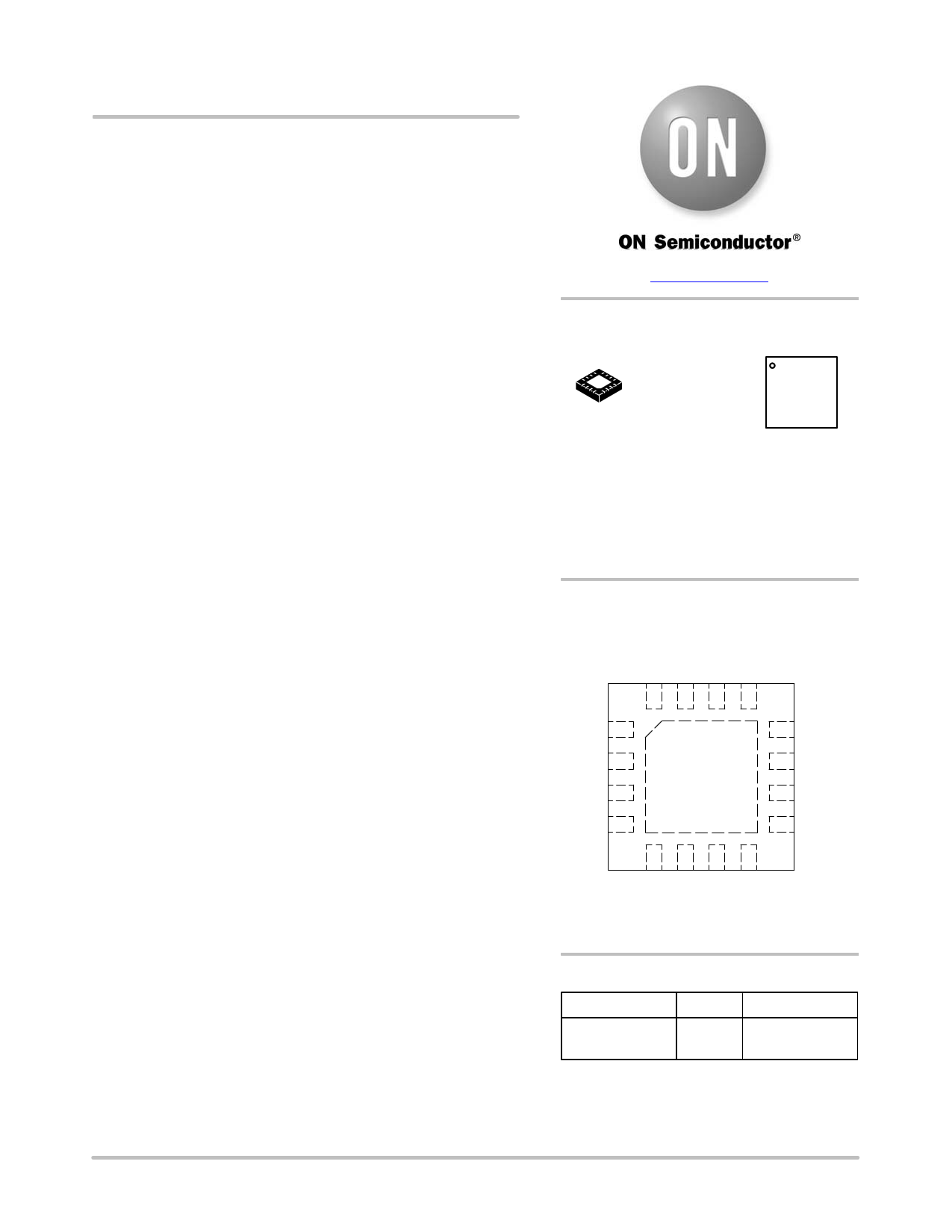
PIN CONNECTIONS
16 15 14 13
VCCP 1
LG 2
LX 3
BOOT 4
12 CSN/VO
11 FBG
10 VSEN
9 FB
5678
(Top View)
ORDERING INFORMATION
Device
Package
Shipping
NCP81147MNTXG QFN16 3000 / Tape & Reel
(Pb−Free)
†For information on tape and reel specifications,
including part orientation and tape sizes, please
refer to our Tape and Reel Packaging Specification
Brochure, BRD8011/D.
© Semiconductor Components Industries, LLC, 2014
August, 2016 − Rev. 1
1
Publication Order Number:
NCP81147/D
1 page 
NCP81147
ELECTRICAL CHARACTERISTICS Unless otherwise stated: −40°C < TA < 85°C; 4.5 V < VCC < 13.2 V; CVCC = 0.1 mF
Parameter
Test Conditions
Min Typ Max
OSCILLATOR (with no ROSC Resistor Defaults to 200 kHz)
Switching Frequency Accuracy
OSC Gain (Note 1)
ROSC open
−15
10
15
Disable threshold
MODULATORS (PWM Comparators)
Minimum Pulse Width
Minimum Turn Off Time (LG on)
Magnitude of the PWM Ramp
Maximum Duty Cycle
Minimum Skip mode frequency
SOFT−START
Soft Start Time @ 200 kHz
SOFT−OFF
Soft OFF bleeding resistor
OVER CURRENT PROTECTION
First Over Current Threshold
Second Over Current Threshold
SYNC PIN
Synchronization Input
Synchronization Input
PROTECTION AND PGOOD
Output Voltage
OVP Threshold
UVP Threshold
Unlatched Overvoltage Threshold
Power Good High Delay (Note 1)
Power Good Low Delay (Note 1)
ZERO CURRENT DETECTION (LX Pin)
Blanking Time before Zero Current
Detection (Note 1)
Capture Time for LX Voltage (Note 1)
Negative LX detection voltage
Positive LX detection voltage
Time for Vth adjustment and settling time
(Note 1)
ROSC/EN pin, Vdis_th
Fsw = 200 kHz, OSC open
Fsw = 200 kHz, OSC open
VIN = 5 V or 12 V
OSC/EN = OPEN
In light load, maximum time for LG to turn on
after HG turns off
0.75
90
250 350 450
1.50
80 95
30
1024 clock cycles, OSC/EN open
5.12
Rdis
CSP−CSN, 4xMasking
CSP−CSN, Immediate action
120
17 20 23
30
VIL, square wave
VIH, square wave
1.0
2.5
Logic Low, Sinking 4 mA
VSEN rising above 1.25 * Vref
VSEN falling below 0.75 * Vref
Vth_disoff with respect to 0.5 Vref
0.4
110 125 140
70 75 80
40 50 60
50
1
Blanking Time after LG is < 1.0 V
40
Time to capture LX voltage once LG is < 1.0 V
(must be within dead time limits)
20
Vbdls
Vbdhs
300 kHz
150 300 450
0.2 0.5 1.0
3.0 3.7
Unit
%
kHz /
mA
V
ns
ns
V
%
kHz
ms
W
mV
mV
V
V
V
%
%
%
ms
ms
ns
ns
mV
V
ms
Initial Negative Current Detection
Threshold Voltage Set Point (Note 1)
LX−GND, Includes ± 2 mV Offset Range
1.0 mV
Vth adjustable Range (Note 1)
−16 0
15 mV
1. Guaranteed by design.
2. For propagation delays, ”tpdh” refers to the specified signal going high ”tpdl” refers to it going low. Reference Gate Timing Diagram.
www.onsemi.com
5
5 Page 
NCP81147
PWR
ON
Yes
EN> Vdis_th
No
VCC> POR &
VCCDR > UVLO _VCCDR (16−
pin )
UV (after Vout reaches UV
threshold in softstart )
UVP
PreOVP detection
VSEN >OV Vth
BG on
VCC > POR &
VCCDR > U_VLO VCCDR
No BOOT >UVLO_BOOT
Yes
Fosc detection
Soft Start ,
Normal Operation
OCP, OVP, UVP detection
OV
OVP
OC
OCP
4 times
reentry
TG OFF, BG
OFF
PGOOD= 0
No
TG OFF, BG ON
PGOOD =0
Vout < Vth_disoff
Yes
After 4 times reentry for
1st threshod
or immediately over 2nd
threshold
TG OFF, BG
OFF
Yes
OVP
No
Vo discharge
mode
Vcc<UVLO_Vcc, Or
EN<Vdis_th Or
Boot<UVLO_Boot
No
Figure 8. State Diagram
www.onsemi.com
11
11 Page | ||
| Páginas | Total 12 Páginas | |
| PDF Descargar | [ Datasheet NCP81147.PDF ] | |
Hoja de datos destacado
| Número de pieza | Descripción | Fabricantes |
| NCP81140 | Multiple-Phase Controller | ON Semiconductor |
| NCP81141 | Single-Phase Controller | ON Semiconductor |
| NCP81142 | Multiple-Phase Controller | ON Semiconductor |
| NCP81143 | Multiple-Phase Controller | ON Semiconductor |
| Número de pieza | Descripción | Fabricantes |
| SLA6805M | High Voltage 3 phase Motor Driver IC. |
Sanken |
| SDC1742 | 12- and 14-Bit Hybrid Synchro / Resolver-to-Digital Converters. |
Analog Devices |
|
DataSheet.es es una pagina web que funciona como un repositorio de manuales o hoja de datos de muchos de los productos más populares, |
| DataSheet.es | 2020 | Privacy Policy | Contacto | Buscar |