|
|
|
PDF NCP4208 Data sheet ( Hoja de datos )
| Número de pieza | NCP4208 | |
| Descripción | VR11.1 Digital Programmable 8-Phase Synchronous Buck Converter | |
| Fabricantes | ON Semiconductor | |
| Logotipo | ||
Hay una vista previa y un enlace de descarga de NCP4208 (archivo pdf) en la parte inferior de esta página. Total 30 Páginas | ||
|
No Preview Available !
NCP4208
VR11.1 Digital
Programmable 8-Phase
Synchronous Buck
Converter with I2C
Interface
The NCP4208 is an integrated power control IC with an I2C interface.
The NCP4208 is a highly efficient, multiphase, synchronous buck
switching regulator controller, which aids design of High Efficiency and
High Density solutions. The NCP4208 can be programmed for 1−, 2−,
3−, 4−, 5−, 6−, 7− or 8−phase operation, allowing for the construction of
up to 8 complementary buck switching stages.
The NCP4208 supports PSI, which is a power state indicator and
can be used to reduce the number of operating phases at light loads.
The I2C interface enables digital programming of key system
parameters to optimize system performance and provide feedback to
the system.
The NCP4208 has a built in shunt regulator that allows the part to be
powered from the +12 V system supply through a series resistor. The
NCP4208 is specified over the extended commercial temperature
range of 0°C to +85°C and is available in a 48 Lead QFN package.
Features
• Selectable 1−, 2−, 3−, 4−, 5−, 6−, 7− or 8−Phase Operation at
Up to 1.5 MHz per Phase
• Temperature Measurement
• Logic−Level PWM Outputs for Interface to External High
Power Drivers
• Fast−Enhanced PWM for Excellent Load Transient Performance
• Active Current Balancing Between All Output Phases
• Built−In Power−Good/Crowbar Blanking Supports
On−The−Fly (OTF) VID Code Changes
• Digitally Programmable 0.375 V to 1.6 V Output Supports
VR11.1 Specifications
• Short Circuit Protection with Latchoff Delay
• Supports PSI Power Saving Mode During Light Loads
• This is a Pb−Free Device
Applications
• Desktop PC
• Servers
© Semiconductor Components Industries, LLC, 2013
September, 2013 − Rev. 5
1
http://onsemi.com
1 48
QFN 48
CASE 485AJ
MARKING DIAGRAM
NCP4208
AWLYYWWG
A = Assembly Lot
WL = Wafer Lot
YY = Year
WW = Work Week
G = Pb−Free Package
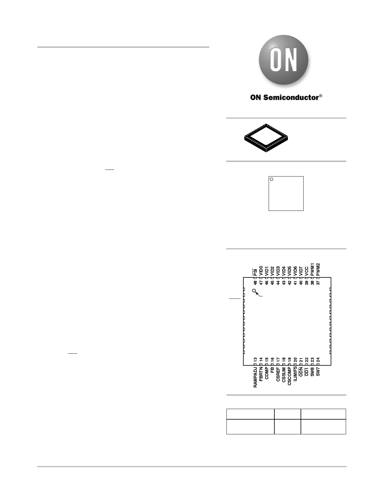
PIN ASSIGNMENT
VCC3 1
PWRDG 2
ALERT 3
SDA 4
SCL 5
EN 6
GND 7
NC 8
NC 9
IMON 10
IREF 11
RT 12
PIN 1
INDICATOR
NCP4208
TOP VIEW
36 PWM3
35 PWM4
34 PWM5
33 PWM6
32 PWM7
31 PWM8
30 SW1
29 SW2
28 SW3
27 SW4
26 SW5
25 SW6
ORDERING INFORMATION
Device
NCP4208MNR2G
Package
Shipping†
QFN48 2500/Tape & Reel
(Pb−Free)
†For information on tape and reel specifications,
including part orientation and tape sizes, please
refer to our Tape and Reel Packaging Specifications
Brochure, BRD8011/D.
Publication Order Number:
NCP4208/D
1 page 
NCP4208
PIN ASSIGNMENT
Pin No.
1
Mnemonic
VCC3
2 PWRGD
3 ALERT
4 SDA
5 SCL
6 EN
7 GND
8 to 9
10
11
NC
IMON
IREF
12 RT
13 RAMPADJ
14 FBRTN
15 COMP
16 FB
17 CSREF
18 CSSUM
19 CSCOMP
20 ILIMFS
21 ODN
22 OD1
23 to 30
31 to 38
SW8 to SW1
PWM8 to PWM1
39
40 to 47
48
VCC
VID7 to VID0
PSI
Description
3.3 V Power Supply Output. A capacitor from this pin to ground provided decoupling for the
interval 3.3 V LDO.
Power−Good Output: Open−drain output that signals when the output voltage is outside of the
proper operating range.
ALERT Output: Open drain output that asserts low when the VR exceeds a programmable limit.
Can be configured for Comparator Mode or Interrupt Mode.
Digital Input / Output. I2C serial data bidirectional pin. Requires pullup.
Digital Input. I2C serial bus clock open drain input. Requires pullup.
Power Supply Enable Input. Pulling this pin to GND disables the PWM outputs and pulls the
PWRGD output low.
Ground. All internal biasing and the logic output signals of the device are referenced to this
ground.
No Connect
Total Current Output Pin.
Current Reference Input. An external resistor from this pin to ground sets the reference current for
IFB, and IILIMFS.
Frequency Setting Resistor Input. An external resistor connected between this pin and GND
sets the oscillator frequency of the device.
PWM Ramp Current Input. An external resistor from the converter input voltage to this pin sets
the internal PWM ramp.
Feedback Return. VID DAC and error amplifier reference for remote sensing of the output
voltage.
Error Amplifier Output and Compensation Point.
Feedback Input. Error amplifier input for remote sensing of the output voltage. An external
resistor between this pin and the output voltage sets the no load offset point.
Current Sense Reference Voltage Input. The voltage on this pin is used as the reference for the
current sense amplifier and the power−good and crowbar functions. This pin should be
connected to the common point of the output inductors.
Current Sense Summing Node. External resistors from each switch node to this pin sum the
average inductor currents together to measure the total output current.
Current Sense Compensation Point. A resistor and capacitor from this pin to CSSUM
determines the gain of the current sense amplifier and the positioning loop response time.
Current Sense and Limit Scaling Pin. An external resistor from this pin to CSCOMP sets the
internal current sensing signal for current limit and IMON. This value can be overwritten using
the I2C interface.
Output Disable Logic Output for PSI operation. This pin is actively pulled low when PSI is low,
otherwise it functions in the same way as OD1.
Output Disable Logic Output. This pin is actively pulled low when the EN input is low or when
VCC is below its UVLO threshold to signal to the Driver IC that the driver high−side and
low−side outputs should go low.
Current Balance Inputs. Inputs for measuring the current level in each phase. The SW pins of
unused phases should be left open.
Logic−Level PWM Outputs. Each output is connected to the input of an external MOSFET driver
such as the ADP3121. Connecting the PWM8, PWM7, PWM6, PWM5, PWM4, PWM3 and
PWM2 outputs to VCC causes that phase to turn off, allowing the NCP4208 to operate as a
1−, 2−, 3−, 4−, 5−, 6−, 7−, or 8−phase controller.
Supply Voltage for the Device. A 340 W resistor should be placed between the 12 V system
supply and the VCC pin. The internal shunt regulator maintains VCC = 5.0 V.
Voltage Identification DAC Inputs. These eight pins are pulled down to GND, providing a logic
zero if left open. When in normal operation mode, the DAC output programs the FB regulation
voltage from 0.375 V to 1.6 V.
Power State Indicator. Pulling this pin low places the controller in lower power state operation.
http://onsemi.com
5
5 Page 
NCP4208
a 2−phase controller connect PWM3, PWM4, PWM5,
PWM6, PWM7 and PWM8 to VCC. To operate as a 1−phase
controller connect PWM2, PWM3, PWM4, PWM5,
PWM6, PWM7 and PWM8 to VCC.
Prior to soft−start, while EN is low, the PWM8, PWM7,
PWM6, PWM5, PWM4, PWM3 and PWM2 pins sink
approximately 100 mA each. An internal comparator checks
each pin’s voltage vs. a threshold of 3.0 V. If the pin is tied
to VCC, it is above the threshold. Otherwise, an internal
current sink pulls the pin to GND, which is below the
threshold. PWM1 is low during the phase detection interval
that occurs during the first eight clock cycles of TD2. After
this time, if the remaining PWM outputs are not pulled to
VCC, the 100 mA current sink is removed, and they function
as normal PWM outputs. If they are pulled to VCC, the
100 mA current source is removed, and the outputs are put
into a high impedance state.
The PWM outputs are logic−level devices intended for
driving fast response external gate drivers such as the
ADP3121. Because each phase is monitored independently,
operation approaching 100% duty cycle is possible. In
addition, more than one output can be on at the same time to
allow overlapping phases.
Master Clock Frequency
The clock frequency of the NCP4208 is set with an
external resistor connected from the RT pin to ground. The
frequency follows the graph in Figure 3. To determine the
frequency per phase, the clock is divided by the number of
phases in use. If all phases are in use, divide by 8. If 4 phases
are in use divide by 4.
Output Voltage Differential Sensing
The NCP4208 combines differential sensing with a high
accuracy VID DAC and reference, and a low offset error
amplifier. This maintains a worst−case specification of
±9 mV differential sensing error over its full operating
output voltage and temperature range. The output voltage is
sensed between the FB pin and FBRTN pin. FB is connected
through a resistor, RB, to the regulation point, usually the
remote sense pin of the microprocessor. FBRTN is
connected directly to the remote sense ground point. The
internal VID DAC and precision reference are referenced to
FBRTN, which has a minimal current of 70 mA to allow
accurate remote sensing. The internal error amplifier
compares the output of the DAC to the FB pin to regulate the
output voltage.
Output Current Sensing
The NCP4208 provides a dedicated current sense
amplifier (CSA) to monitor the total output current for
proper voltage positioning vs. load current, for the IMON
output and for current limit detection. Sensing the load
current at the output gives the total real time current being
delivered to the load, which is an inherently more accurate
method than peak current detection or sampling the current
across a sense element such as the low−side MOSFET. This
amplifier can be configured several ways, depending on the
objectives of the system, as follows:
• Output inductor DCR sensing without a thermistor for
lowest cost.
• Output inductor DCR sensing with a thermistor for
improved accuracy with tracking of inductor
temperature.
• Sense resistors for highest accuracy measurements.
The positive input of the CSA is connected to the
CSREF pin, which is connected to the average output
voltage. The inputs to the amplifier are summed together
through resistors from the sensing element, such as the
switch node side of the output inductors, to the inverting
input CSSUM. The feedback resistor between CSCOMP
and CSSUM sets the gain of the amplifier and a filter
capacitor is placed in parallel with this resistor. The gain of
the amplifier is programmable by adjusting the feedback
resistor. This difference signal is used internally to offset the
VID DAC for voltage positioning. This different signal can
be adjusted between 50%−150% of the external value using
the I2C Loadline Calibration (0xDE) and Loadline Set
(0xDF) commands.
The difference between CSREF and CSCOMP is then
used as a differential input for the current limit comparator.
To provide the best accuracy for sensing current, the CSA
is designed to have a low offset input voltage. Also, the
sensing gain is determined by external resistors to make it
extremely accurate.
The CPU current can also be monitored over the I2C
interface. The current limit and the loadline can be
programmed over I2C interface.
Loadline Setting
The Loadline is programmable over the I2C on the
NCP4208. It is programmed using the Loadline Calibration
(0xDE) and Loadline Set (0xDF) commands. The Loadline
can be adjusted between 0% and 100% of the external RCSA.
In this example RCSA = 1 mW. RO needs to be 0.8 mW,
therefore programming the Loadline Calibration + Loadline
Set register to give a combined percentage of 80% will set
the RO to 0.8 mW.
Table 2. Loadline Commands
Code
0 0000
0 0001
1 0000
1 0001
1 1110
1 1111
Loadline (as a percentage of RCSA)
0%
3.226%
51.6% = default
53.3%
96.7%
100%
http://onsemi.com
11
11 Page | ||
| Páginas | Total 30 Páginas | |
| PDF Descargar | [ Datasheet NCP4208.PDF ] | |
Hoja de datos destacado
| Número de pieza | Descripción | Fabricantes |
| NCP4200 | Programmable Multi-Phase Synchronous Buck Converter | ON Semiconductor |
| NCP4201 | Programmable Multi-Phase Synchronous Buck Converter | ON Semiconductor |
| NCP4206 | VR11.1 Digital Programmable Multi-Phase Synchronous Buck Converter | ON Semiconductor |
| NCP4208 | VR11.1 Digital Programmable 8-Phase Synchronous Buck Converter | ON Semiconductor |
| Número de pieza | Descripción | Fabricantes |
| SLA6805M | High Voltage 3 phase Motor Driver IC. |
Sanken |
| SDC1742 | 12- and 14-Bit Hybrid Synchro / Resolver-to-Digital Converters. |
Analog Devices |
|
DataSheet.es es una pagina web que funciona como un repositorio de manuales o hoja de datos de muchos de los productos más populares, |
| DataSheet.es | 2020 | Privacy Policy | Contacto | Buscar |