|
|
|
PDF NCV7754 Data sheet ( Hoja de datos )
| Número de pieza | NCV7754 | |
| Descripción | Octal Low-Side Relay Driver | |
| Fabricantes | ON Semiconductor | |
| Logotipo | ||
Hay una vista previa y un enlace de descarga de NCV7754 (archivo pdf) en la parte inferior de esta página. Total 26 Páginas | ||
|
No Preview Available !
NCV7754
Octal Low-Side
Relay Driver
The NCV7754 is an automotive eight channel low−side driver
providing drive capability up to 500 mA per channel. Output control is
via a SPI port and offers convenient reporting of faults for open load
(or short to ground), over load, and over temperature conditions.
Additionally, parallel control of the outputs is addressable (in pairs)
via the INx pins.
A dedicated limp−home mode pin (LHI) enables OUT1−OUT4
while disabling OUT5−OUT8.
Each output driver is protected for over load current and includes an
output clamp for inductive loads.
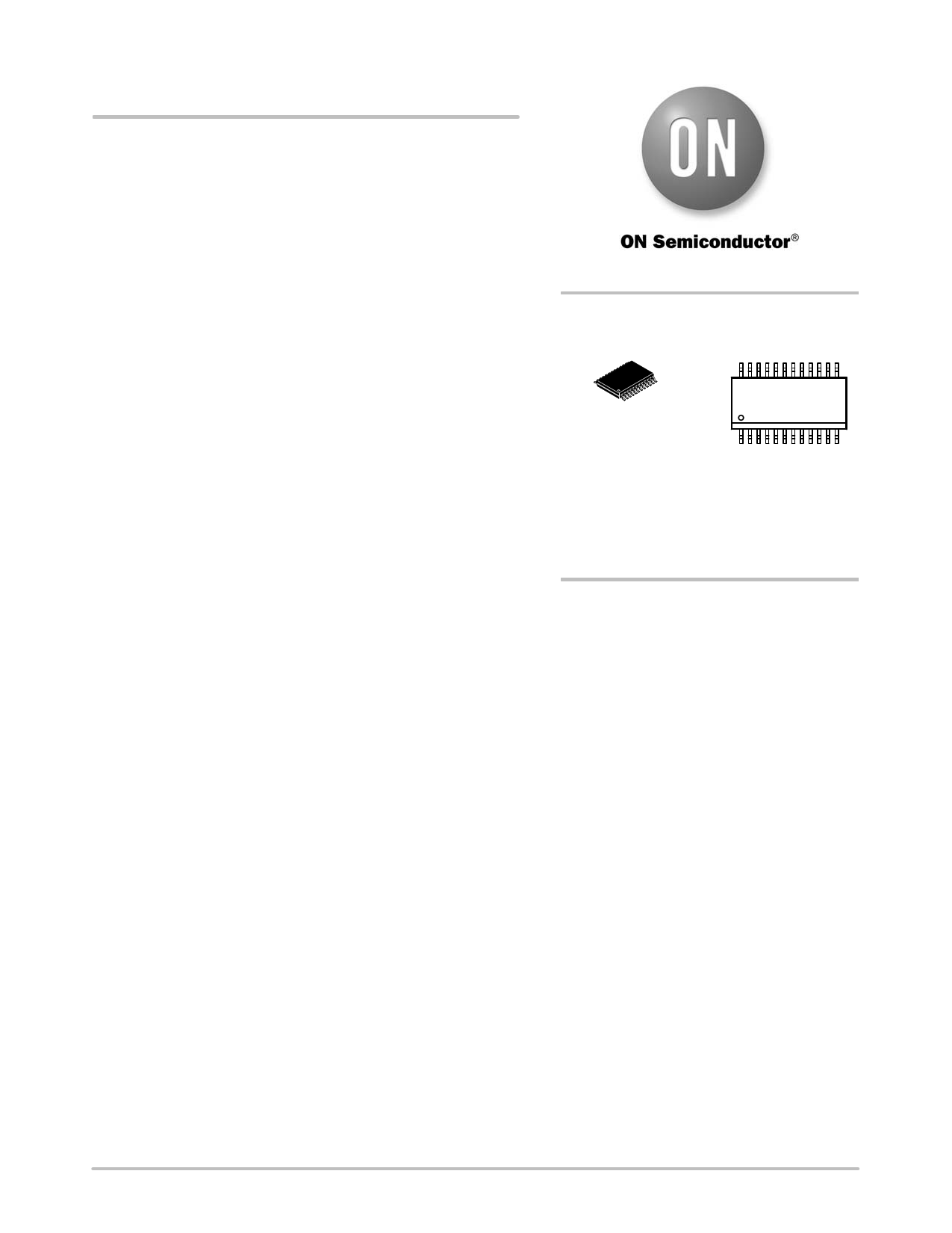
The NCV7754 is available in a SSOP−24 fused lead package.
Features
• 8 Channels
• 500 mA Low−Side Drivers
♦ RDS(on) 0.8 W (Typ), 1.6 W (Max)
• 16−bit SPI Control
♦ Frame Error Detection (8−bit)
♦ Daisy Chain Capable
• Parallel Input Pins for PWM operation
• Power Up Without Open Circuit Detection Active (for LED
applications)
• Low Quiescent Current in Sleep and Standby Modes
• Limp Home Functionality
• 3.3 V and 5 V compatible Digital Input Supply Range
• Fault Reporting
♦ Open Load Detection (selectable)
♦ Over Load
♦ Over Temperature
• Power−on Reset (VDD, VDDA)
• SSOP−24 Package (internally fused leads)
• NCV Prefix for Automotive and Other Applications Requiring
Unique Site and Control Change Requirements; AEC−Q100
Qualified and PPAP Capable
• These are Pb−Free Devices
Applications
• Automotive Body Control Unit
• Automotive Engine Control Unit
• Relay Driver
• LED Driver
• Stepper Motor Driver
http://onsemi.com
MARKING
DIAGRAM
SSOP−24
CASE 565AL
NCV7754
AWLYWWG
A = Assembly Location
WL = Wafer Lot
Y = Year
WW = Work Week
G = Pb−Free Package
ORDERING INFORMATION
See detailed ordering and shipping information in the package
dimensions section on page 25 of this data sheet.
© Semiconductor Components Industries, LLC, 2015
February, 2015 − Rev. 1
1
Publication Order Number:
NCV7754/D
1 page 
NCV7754
MAXIMUM RATINGS
Parameter
Supply Input Voltage (VDDA, VDD)
DC
Digital I/O pin voltage
(EN, LHI, Inx, CSB, SCLK, SI)
(SO)
High Voltage Pins (OUTx)
DC
Peak Transient
Output Current (OUTx)
Clamping Energy
Maximum (single pulse)
Repetitive (multiple pulse) (Note 2)
Operating Junction Temperature Range
Storage Temperature Range
ESD Capability − (AEC−Q100−002)
Human body model (100 pF, 1.5 kW) (OUTx pins)
Human body model (100 pF, 1.5 kW) (all other pins)
ESD Capability − (AEC−Q100−003)
Machine Model (200 pF)
AECQ10x−12−RevA
Short Circuit Reliability Characterization
Min
−0.3
−0.3
−0.3
−0.3
−1
−
−
−40
−55
−4000
−2000
−200
Max
5.5
5.5
VDD + 0.3
36
44 (Note 1)
0.95
85
−
150
150
4000
2000
200
Unit
V
V
V
A
mJ
°C
°C
V
V
Grade A
−
PACKAGE
Moisture Sensitivity Level
Lead Temperature Soldering: SMD style only, Reflow (Note 3)
Pb−Free Part 60 − 150 sec above 217°C, 40 sec max at peak
MSL2
265 peak
−
°C
Package Thermal Resistance (per JESD51)
°C/W
SSOP−24
Junction−to−Ambient (1s0p + 600 mm2 Cu) (Note 4)
Junction−to−Ambient (2s2p) (Notes 4 and 5)
Junction−to−Pin (pins 1, 2, 11, 12) (Note 6)
68
62
30
Stresses exceeding Maximum Ratings may damage the device. Maximum Ratings are stress ratings only. Functional operation above the
Recommended Operating Conditions is not implied. Extended exposure to stresses above the Recommended Operating Conditions may affect
device reliability.
1. Internally limited. Specification applies to unpowered and powered modes. (0 V to VDDA, 0 V to VDD)
2. Testing particulars, 2M pulses, Vbat = 15 V, 63 W, 390 mH, TA = 25°C. (See Figure 4)
3. For additional information, see or download ON Semiconductor’s Soldering and Mounting Techniques Reference Manual, SOLDERRM/D
and Application Note AND8083/D.
4. 76 mm x 76 mm x 1.5 mm FR4 PCB with additional heat spreading copper (2 oz) of 600 mm2, LS1 to LS8 dissipating 100 mW each. No vias.
5. Include 2 inner 1 oz copper layers. No vias.
6. One output dissipating 100 mW.
Figure 4. Repetitive Clamping Energy Test
http://onsemi.com
5
5 Page 
NCV7754
TYPICAL PERFORMANCE GRAPHS
1.0
0.9
0.8
0.7
0.6
0.5
0.4
0.3
0.2
0.1 IOUT = −180 mA
0
−40 −20 0 20 40 60 80 100 120 140
TEMPERATURE (°C)
Figure 18. Output Body Diode Voltage vs.
Temperature
http://onsemi.com
11
11 Page | ||
| Páginas | Total 26 Páginas | |
| PDF Descargar | [ Datasheet NCV7754.PDF ] | |
Hoja de datos destacado
| Número de pieza | Descripción | Fabricantes |
| NCV7751 | Twelve Low-Side Relay Drivers | ON Semiconductor |
| NCV7751DQR2G | Twelve Low-Side Relay Drivers | ON Semiconductor |
| NCV7754 | Octal Low-Side Relay Driver | ON Semiconductor |
| Número de pieza | Descripción | Fabricantes |
| SLA6805M | High Voltage 3 phase Motor Driver IC. |
Sanken |
| SDC1742 | 12- and 14-Bit Hybrid Synchro / Resolver-to-Digital Converters. |
Analog Devices |
|
DataSheet.es es una pagina web que funciona como un repositorio de manuales o hoja de datos de muchos de los productos más populares, |
| DataSheet.es | 2020 | Privacy Policy | Contacto | Buscar |