|
|
|
PDF NVMD6N04R2G Data sheet ( Hoja de datos )
| Número de pieza | NVMD6N04R2G | |
| Descripción | Power MOSFET ( Transistor ) | |
| Fabricantes | ON Semiconductor | |
| Logotipo | ||
Hay una vista previa y un enlace de descarga de NVMD6N04R2G (archivo pdf) en la parte inferior de esta página. Total 5 Páginas | ||
|
No Preview Available !
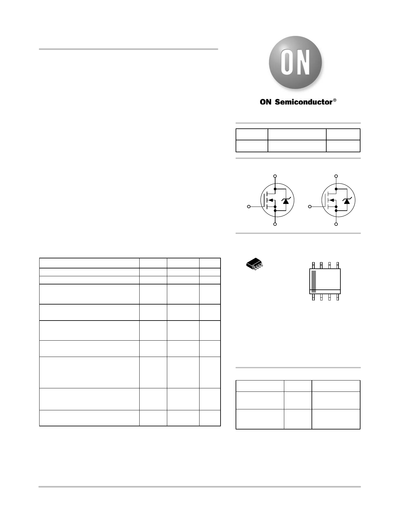
NTMD6N04, NVMD6N04
Power MOSFET
40 V, 5.8 A, Dual N−Channel SOIC−8
Features
• Designed for use in low voltage, high speed switching applications
• Ultra Low On−Resistance Provides
Higher Efficiency and Extends Battery Life
− RDS(on) = 0.027 W, VGS = 10 V (Typ)
− RDS(on) = 0.034 W, VGS = 4.5 V (Typ)
• Miniature SOIC−8 Surface Mount Package Saves Board Space
• Diode is Characterized for Use in Bridge Circuits
• Diode Exhibits High Speed, with Soft Recovery
• NVMD Prefix for Automotive and Other Applications Requiring
Unique Site and Control Change Requirements; AEC−Q101
Qualified and PPAP Capable*
• These Devices are Pb−Free and are RoHS Compliant
Applications
• DC−DC Converters
• Computers
• Printers
• Cellular and Cordless Phones
• Disk Drives and Tape Drives
MAXIMUM RATINGS (TJ = 25°C unless otherwise noted)
Rating
Symbol
Value
Unit
Drain−to−Source Voltage
Gate−to−Source Voltage − Continuous
Drain Current (Note 1)
− Continuous @ TA = 25°C
− Single Pulse (tp ≤ 10 ms)
Drain Current (Note 2)
− Continuous @ TA = 25°C
Total Power Dissipation
@ TA = 25°C (Note 1)
@ TA = 25°C (Note 2)
Operating and Storage Temperature
Range
VDSS
VGS
ID
IDM
ID
40
"20
5.8
29
4.6
V
V
Adc
Apk
Adc
PD
TJ, Tstg
2.0
1.29
−55 to +150
W
°C
Single Pulse Drain−to−Source Avalanche
Energy − Starting TJ = 25°C
(VDD = 40 Vdc, VGS = 5.0 Vdc,
Vdc, Peak IL = 7.0 Apk,
L = 10 mH, RG = 25 W)
Thermal Resistance
− Junction−to−Ambient (Note 1)
− Junction−to−Ambient (Note 2)
EAS
RqJA
245 mJ
°C/W
62.5
97
Maximum Lead Temperature for
Soldering Purposes for 10 Sec
TL 260 °C
Stresses exceeding Maximum Ratings may damage the device. Maximum
Ratings are stress ratings only. Functional operation above the Recommended
Operating Conditions is not implied. Extended exposure to stresses above the
Recommended Operating Conditions may affect device reliability.
1. When surface mounted to an FR4 board using 1″ pad size, t ≤ 10 s
2. When surface mounted to an FR4 board using 1″ pad size, t = steady state
http://onsemi.com
VDSS
40 V
RDS(ON) Typ
27 mW @ VGS = 10 V
ID Max
5.8 A
N−Channel
D
D
GG
SS
8
1
SOIC−8
CASE 751
STYLE 11
MARKING DIAGRAM &
PIN ASSIGNMENT
D1 D1 D2 D2
8
E6N04
AYWW G
G
1
S1 G1 S2 G2
E6N04 = Specific Device Code
A = Assembly Location
Y = Year
WW = Work Week
G = Pb−Free Package
(Note: Microdot may be in either location)
ORDERING INFORMATION
Device
Package
Shipping†
NTMD6N04R2G
NVMD6N04R2G*
SOIC−8
(Pb−Free)
SOIC−8
(Pb−Free)
2500 / Tape &
Reel
2500 / Tape &
Reel
†For information on tape and reel specifications,
including part orientation and tape sizes, please
refer to our Tape and Reel Packaging Specification
Brochure, BRD8011/D.
© Semiconductor Components Industries, LLC, 2013
August, 2013 − Rev. 2
1
Publication Order Number:
NTMD6N04R2/D
1 page 
NTMD6N04, NVMD6N04
PACKAGE DIMENSIONS
−X−
A
SOIC−8 NB
CASE 751−07
ISSUE AK
B
−Y−
−Z−
H
85
S 0.25 (0.010) M Y M
1
4
K
G
D
C
SEATING
PLANE
N X 45_
0.10 (0.004)
M
J
0.25 (0.010) M Z Y S X S
SOLDERING FOOTPRINT*
1.52
0.060
7.0
0.275
4.0
0.155
NOTES:
1. DIMENSIONING AND TOLERANCING PER
ANSI Y14.5M, 1982.
2. CONTROLLING DIMENSION: MILLIMETER.
3. DIMENSION A AND B DO NOT INCLUDE
MOLD PROTRUSION.
4. MAXIMUM MOLD PROTRUSION 0.15 (0.006)
PER SIDE.
5. DIMENSION D DOES NOT INCLUDE DAMBAR
PROTRUSION. ALLOWABLE DAMBAR
PROTRUSION SHALL BE 0.127 (0.005) TOTAL
IN EXCESS OF THE D DIMENSION AT
MAXIMUM MATERIAL CONDITION.
6. 751−01 THRU 751−06 ARE OBSOLETE. NEW
STANDARD IS 751−07.
MILLIMETERS
INCHES
DIM MIN MAX MIN MAX
A 4.80 5.00 0.189 0.197
B 3.80 4.00 0.150 0.157
C 1.35 1.75 0.053 0.069
D 0.33 0.51 0.013 0.020
G 1.27 BSC 0.050 BSC
H 0.10 0.25 0.004 0.010
J 0.19 0.25 0.007 0.010
K 0.40 1.27 0.016 0.050
M 0_ 8_ 0_ 8_
N 0.25 0.50 0.010 0.020
S 5.80 6.20 0.228 0.244
STYLE 11:
PIN 1. SOURCE 1
2. GATE 1
3. SOURCE 2
4. GATE 2
5. DRAIN 2
6. DRAIN 2
7. DRAIN 1
8. DRAIN 1
0.6
0.024
1.270
0.050
ǒ ǓSCALE 6:1
mm
inches
*For additional information on our Pb−Free strategy and soldering
details, please download the ON Semiconductor Soldering and
Mounting Techniques Reference Manual, SOLDERRM/D.
ON Semiconductor and
are registered trademarks of Semiconductor Components Industries, LLC (SCILLC). SCILLC reserves the right to make changes without further notice
to any products herein. SCILLC makes no warranty, representation or guarantee regarding the suitability of its products for any particular purpose, nor does SCILLC assume any liability
arising out of the application or use of any product or circuit, and specifically disclaims any and all liability, including without limitation special, consequential or incidental damages.
“Typical” parameters which may be provided in SCILLC data sheets and/or specifications can and do vary in different applications and actual performance may vary over time. All
operating parameters, including “Typicals” must be validated for each customer application by customer’s technical experts. SCILLC does not convey any license under its patent rights
nor the rights of others. SCILLC products are not designed, intended, or authorized for use as components in systems intended for surgical implant into the body, or other applications
intended to support or sustain life, or for any other application in which the failure of the SCILLC product could create a situation where personal injury or death may occur. Should
Buyer purchase or use SCILLC products for any such unintended or unauthorized application, Buyer shall indemnify and hold SCILLC and its officers, employees, subsidiaries, affiliates,
and distributors harmless against all claims, costs, damages, and expenses, and reasonable attorney fees arising out of, directly or indirectly, any claim of personal injury or death
associated with such unintended or unauthorized use, even if such claim alleges that SCILLC was negligent regarding the design or manufacture of the part. SCILLC is an Equal
Opportunity/Affirmative Action Employer. This literature is subject to all applicable copyright laws and is not for resale in any manner.
PUBLICATION ORDERING INFORMATION
LITERATURE FULFILLMENT:
Literature Distribution Center for ON Semiconductor
P.O. Box 5163, Denver, Colorado 80217 USA
Phone: 303−675−2175 or 800−344−3860 Toll Free USA/Canada
Fax: 303−675−2176 or 800−344−3867 Toll Free USA/Canada
Email: [email protected]
N. American Technical Support: 800−282−9855 Toll Free
USA/Canada
Europe, Middle East and Africa Technical Support:
Phone: 421 33 790 2910
Japan Customer Focus Center
Phone: 81−3−5817−1050
http://onsemi.com
5
ON Semiconductor Website: www.onsemi.com
Order Literature: http://www.onsemi.com/orderlit
For additional information, please contact your local
Sales Representative
NTMD6N04R2/D
5 Page | ||
| Páginas | Total 5 Páginas | |
| PDF Descargar | [ Datasheet NVMD6N04R2G.PDF ] | |
Hoja de datos destacado
| Número de pieza | Descripción | Fabricantes |
| NVMD6N04R2G | Power MOSFET ( Transistor ) | ON Semiconductor |
| Número de pieza | Descripción | Fabricantes |
| SLA6805M | High Voltage 3 phase Motor Driver IC. |
Sanken |
| SDC1742 | 12- and 14-Bit Hybrid Synchro / Resolver-to-Digital Converters. |
Analog Devices |
|
DataSheet.es es una pagina web que funciona como un repositorio de manuales o hoja de datos de muchos de los productos más populares, |
| DataSheet.es | 2020 | Privacy Policy | Contacto | Buscar |