|
|
|
PDF NVD6416AN Data sheet ( Hoja de datos )
| Número de pieza | NVD6416AN | |
| Descripción | N-Channel Power MOSFET / Transistor | |
| Fabricantes | ON Semiconductor | |
| Logotipo | ||
Hay una vista previa y un enlace de descarga de NVD6416AN (archivo pdf) en la parte inferior de esta página. Total 7 Páginas | ||
|
No Preview Available !
NTD6416AN, NVD6416AN
N-Channel Power MOSFET
100 V, 17 A, 81 mW
Features
• Low RDS(on)
• High Current Capability
• 100% Avalanche Tested
• NVD Prefix for Automotive and Other Applications Requiring
Unique Site and Control Change Requirements; AEC−Q101
Qualified and PPAP Capable
• These Devices are Pb−Free and are RoHS Compliant
MAXIMUM RATINGS (TJ = 25°C unless otherwise noted)
Parameter
Symbol Value
Unit
Drain−to−Source Voltage
VDSS
100
V
Gate−to−Source Voltage − Continuous
VGS ±20 V
Continuous Drain
Current
Steady
State
TC = 25°C
TC = 100°C
ID
17 A
11
Power Dissipation
Steady TC = 25°C
State
PD
71 W
Pulsed Drain Current
tp = 10 ms
Operating and Storage Temperature Range
IDM
TJ, Tstg
62
−55 to
+175
A
°C
Source Current (Body Diode)
Single Pulse Drain−to−Source Avalanche
Energy (VDD = 50 Vdc, VGS = 10 Vdc,
IL(pk) = 17 A, L = 0.3 mH, RG = 25 W)
Lead Temperature for Soldering
Purposes, 1/8″ from Case for 10 Seconds
IS 17 A
EAS 43 mJ
TL 260 °C
Stresses exceeding those listed in the Maximum Ratings table may damage the
device. If any of these limits are exceeded, device functionality should not be
assumed, damage may occur and reliability may be affected.
THERMAL RESISTANCE RATINGS
Parameter
Symbol Max Unit
Junction−to−Case (Drain) Steady State
RqJC
Junction−to−Ambient (Note 1)
RqJA
1. Surface mounted on FR4 board using 1 sq in pad size,
(Cu Area 1.127 sq in [2 oz] including traces).
2.1 °C/W
40
http://onsemi.com
V(BR)DSS
100 V
RDS(on) MAX
81 mW @ 10 V
ID MAX
(Note 1)
17 A
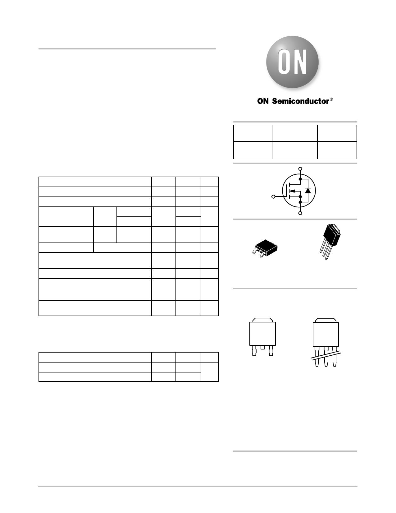
D
N−Channel
G
S
4
4
12
3
DPAK
CASE 369AA
STYLE 2
1
2
3
IPAK
CASE 369D
STYLE 2
MARKING DIAGRAM
& PIN ASSIGNMENTS
4 Drain
4 Drain
1
Gate
2
Drain
3
Source
1
Gate
2
Drain
3
Source
A
Y
WW
6416AN
G
= Assembly Location*
= Year
= Work Week
= Device Code
= Pb−Free Package
* The Assembly Location code (A) is front side
optional. In cases where the Assembly Location is
stamped in the package, the front side assembly
code may be blank.
ORDERING INFORMATION
See detailed ordering and shipping information on page 5 of
this data sheet.
© Semiconductor Components Industries, LLC, 2014
September, 2014 − Rev. 3
1
Publication Order Number:
NTD6416AN/D
1 page 
NTD6416AN, NVD6416AN
TYPICAL CHARACTERISTICS
10
1 D = 0.5
0.2
0.1
0.1
0.05
0.02
0.01
0.01
SINGLE PULSE
0.001
0.000001
0.00001
0.0001
0.001
0.01
0.1
1
10
t, PULSE TIME (s)
Figure 13. Thermal Response
ORDERING INFORMATION
Device
Package
Shipping†
NTD6416ANT4G
DPAK
(Pb−Free)
2500 / Tape & Reel
NTD6416AN−1G
IPAK
(Pb−Free)
75 Units / Rail
NVD6416ANT4G*
DPAK
(Pb−Free)
2500 / Tape & Reel
†For information on tape and reel specifications, including part orientation and tape sizes, please refer to our Tape and Reel Packaging
Specification Brochure, BRD8011/D.
*NVD Prefix for Automotive and Other Applications Requiring Unique Site and Control Change Requirements; AEC−Q101 Qualified and PPAP
Capable.
http://onsemi.com
5
5 Page | ||
| Páginas | Total 7 Páginas | |
| PDF Descargar | [ Datasheet NVD6416AN.PDF ] | |
Hoja de datos destacado
| Número de pieza | Descripción | Fabricantes |
| NVD6416AN | N-Channel Power MOSFET / Transistor | ON Semiconductor |
| NVD6416ANL | N-Channel Power MOSFET / Transistor | ON Semiconductor |
| Número de pieza | Descripción | Fabricantes |
| SLA6805M | High Voltage 3 phase Motor Driver IC. |
Sanken |
| SDC1742 | 12- and 14-Bit Hybrid Synchro / Resolver-to-Digital Converters. |
Analog Devices |
|
DataSheet.es es una pagina web que funciona como un repositorio de manuales o hoja de datos de muchos de los productos más populares, |
| DataSheet.es | 2020 | Privacy Policy | Contacto | Buscar |