|
|
PDF 74CBTLV3245 Data sheet ( Hoja de datos )
| Número de pieza | 74CBTLV3245 | |
| Descripción | 8-bit bus | |
| Fabricantes | NXP Semiconductors | |
| Logotipo | ||
Hay una vista previa y un enlace de descarga de 74CBTLV3245 (archivo pdf) en la parte inferior de esta página. Total 18 Páginas | ||
|
No Preview Available !
74CBTLV3245
8-bit bus switch with output enable
Rev. 2 — 15 December 2011
Product data sheet
1. General description
The 74CBTLV3245 is an 8-pole, single-throw bus switch. The device features a single
output enable input (OE) that controls eight switch channels. The switches are disabled
when OE is HIGH. Schmitt-trigger action at control inputs makes the circuit tolerant of
slower input rise and fall times. This device is fully specified for partial power-down
applications using IOFF. The IOFF circuitry disables the output, preventing the damaging
backflow current through the device when it is powered down.
2. Features and benefits
Supply voltage range from 2.3 V to 3.6 V
High noise immunity
Complies with JEDEC standard:
JESD8-5 (2.3 V to 2.7 V)
JESD8-B/JESD36 (2.7 V to 3.6 V)
ESD protection:
HBM JESD22-A114F exceeds 2000 V
MM JESD22-A115-A exceeds 200 V
CDM AEC-Q100-011 revision B exceeds 1000 V
5 switch connection between two ports
Rail to rail switching on data I/O ports
CMOS low power consumption
Latch-up performance exceeds 250 mA per JESD78B Class I level A
IOFF circuitry provides partial Power-down mode operation
Multiple package options
Specified from 40 C to +85 C and 40 C to +125 C
1 page 
NXP Semiconductors
74CBTLV3245
8-bit bus switch with output enable
8. Recommended operating conditions
Table 5.
Symbol
VCC
VI
VSW
Tamb
t/V
Recommended operating conditions
Parameter
Conditions
supply voltage
input voltage
switch voltage
enable and disable mode
ambient temperature
input transition rise and fall rate VCC = 2.3 V to 3.6 V
[1] Applies to control signal levels.
9. Static characteristics
Min
2.3
0
0
40
[1] -
Max
3.6
3.6
VCC
+125
200
Unit
V
V
V
C
ns/V
Table 6. Static characteristics
At recommended operating conditions voltages are referenced to GND (ground = 0 V).
Symbol Parameter
Conditions
Tamb = 40 C to +85 C
Min Typ[1] Max
VIH
VIL
II
IS(OFF)
HIGH-level
input voltage
VCC = 2.3 V to 2.7 V
VCC = 3.0 V to 3.6 V
LOW-level input VCC = 2.3 V to 2.7 V
voltage
VCC = 3.0 V to 3.6 V
input leakage
current
pin OE; VI = GND to VCC;
VCC = 3.6 V
OFF-state
VCC = 3.6 V; see Figure 6
leakage current
1.7 -
-
2.0 -
-
- - 0.7
- - 0.9
- - 1
- - 1
IS(ON)
ON-state
VCC = 3.6 V; see Figure 7
leakage current
- - 1
IOFF
ICC
ICC
CI
CS(OFF)
power-off
leakage current
supply current
additional
supply current
input
capacitance
OFF-state
capacitance
VI or VO = 0 V to 3.6 V;
VCC = 0 V
VI = GND or VCC; IO = 0 A;
VSW = GND or VCC;
VCC = 3.6 V
pin OE; VI = VCC 0.6 V;
VSW = GND or VCC;
VCC = 3.6 V
pin OE; VCC = 3.3 V;
VI = 0 V to 3.3 V
VCC = 3.3 V; VI = 0 V to 3.3 V
[2]
-
-
-
-
-
- 10
- 10
- 300
0.9 -
5.2 -
CS(ON) ON-state
capacitance
VCC = 3.3 V; VI = 0 V to 3.3 V
- 14.3 -
Tamb = 40 C to +125 C Unit
Min Max
1.7 - V
2.0 - V
- 0.7 V
- 0.9 V
- 20 A
- 20 A
- 20 A
- 50 A
- 50 A
- 2000 A
- - pF
- - pF
- - pF
[1] All typical values are measured at Tamb = 25 C.
[2] One input at 3 V, other inputs at VCC or GND.
74CBTLV3245
Product data sheet
All information provided in this document is subject to legal disclaimers.
Rev. 2 — 15 December 2011
© NXP B.V. 2011. All rights reserved.
5 of 18
5 Page 
NXP Semiconductors
74CBTLV3245
8-bit bus switch with output enable
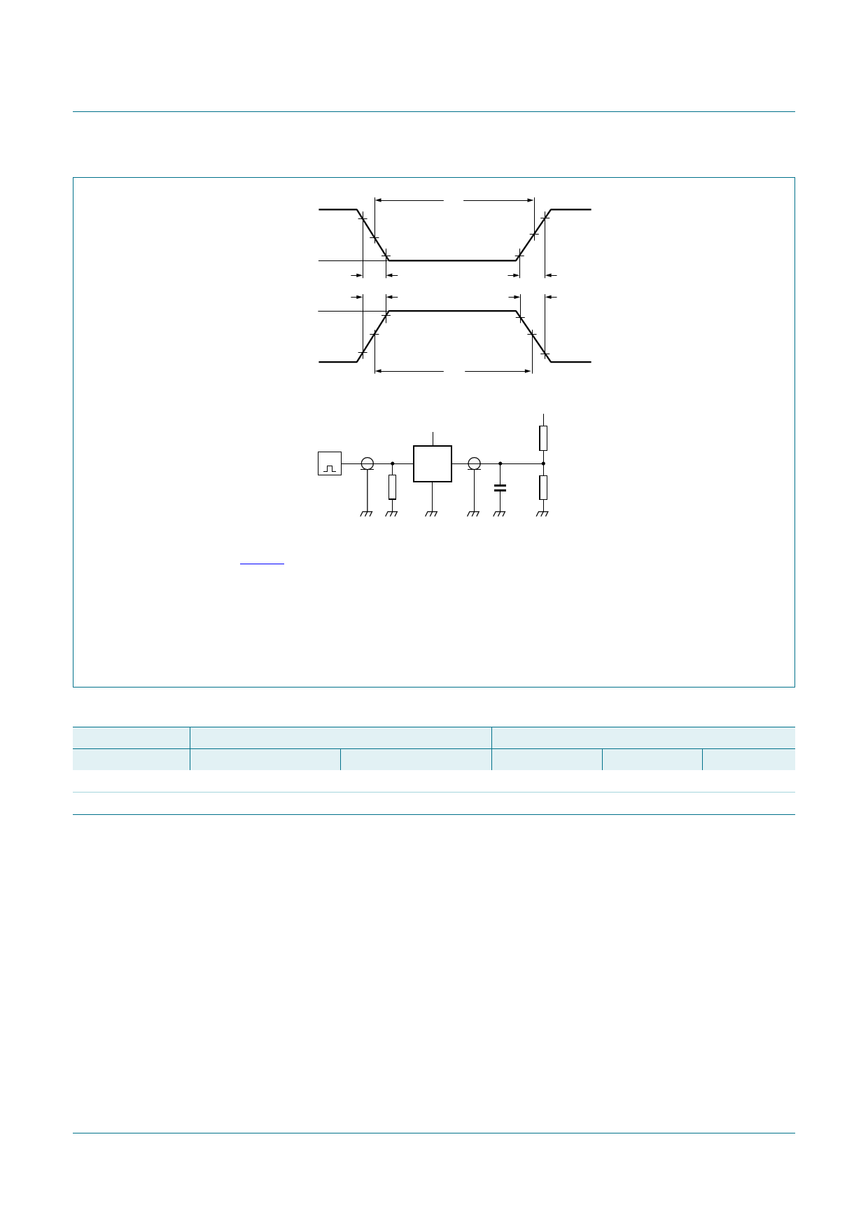
VI
negative
pulse
0V
VI
positive
pulse
0V
90 %
10 %
VM
10 %
tf
tr
90 %
VM
tW
tW
VM
tr
tf
VM
VI
G
VCC
DUT
VO
VEXT
RL
RT CL RL
001aae331
Test data is given in Table 10.
Definitions for test circuit:
RL = Load resistance.
CL = Load capacitance including jig and probe capacitance.
RT = Termination resistance should be equal to the output impedance Zo of the pulse generator.
VEXT = External voltage for measuring switching times.
Fig 17. Test circuit for measuring switching times
Table 10. Test data
Supply voltage Load
VCC
2.3 V to 2.7 V
CL
30 pF
3.0 V to 3.6 V
50 pF
RL
500
500
VEXT
tPLH, tPHL
open
open
tPZH, tPHZ
GND
GND
tPZL, tPLZ
2VCC
2VCC
74CBTLV3245
Product data sheet
All information provided in this document is subject to legal disclaimers.
Rev. 2 — 15 December 2011
© NXP B.V. 2011. All rights reserved.
11 of 18
11 Page | ||
| Páginas | Total 18 Páginas | |
| PDF Descargar | [ Datasheet 74CBTLV3245.PDF ] | |
Hoja de datos destacado
| Número de pieza | Descripción | Fabricantes |
| 74CBTLV3245 | 8-bit bus | NXP Semiconductors |
| Número de pieza | Descripción | Fabricantes |
| SLA6805M | High Voltage 3 phase Motor Driver IC. |
Sanken |
| SDC1742 | 12- and 14-Bit Hybrid Synchro / Resolver-to-Digital Converters. |
Analog Devices |
|
DataSheet.es es una pagina web que funciona como un repositorio de manuales o hoja de datos de muchos de los productos más populares, |
| DataSheet.es | 2020 | Privacy Policy | Contacto | Buscar |
