|
|
|
PDF NTGS3130N Data sheet ( Hoja de datos )
| Número de pieza | NTGS3130N | |
| Descripción | Power MOSFET ( Transistor ) | |
| Fabricantes | ON Semiconductor | |
| Logotipo | ||
Hay una vista previa y un enlace de descarga de NTGS3130N (archivo pdf) en la parte inferior de esta página. Total 6 Páginas | ||
|
No Preview Available !
NTGS3130N, NVGS3130N
Power MOSFET
20 V, 5.6 A Single
N-Channel, TSOP-6
Features
• Leading Edge Trench Technology for Low On Resistance
• Low Gate Charge for Fast Switching
• Small Size (3 x 2.75 mm) TSOP−6 Package
• NV Prefix for Automotive and Other Applications Requiring Unique
Site and Control Change Requirements; AEC−Q101 Qualified and
PPAP Capable
• This is a Pb−Free Device
Applications
• DC−DC Converters
• Lithium Ion Battery Applications
• Load/Power Switching
MAXIMUM RATINGS (TJ = 25°C unless otherwise noted)
Rating
Symbol Value Unit
Drain−to−Source Voltage
Gate−to−Source Voltage
VDSS 20 V
VGS ±8 V
Continuous Drain Current
(Note 1)
Power Dissipation
(Note 1)
Steady
State
t ≤ 10 s
Steady
State
t ≤ 10 s
TA = 25°C
TA = 85°C
TA = 25°C
TA = 25°C
ID
PD
5.6
4.1 A
6.2
1.1
W
1.4
Continuous Drain Current
(Note 2)
Power Dissipation
(Note 2)
Steady
State
TA = 25°C
TA = 85°C
TA = 25°C
ID
PD
4.2
3.0 A
0.6 W
Pulsed Drain Current
tP ≤ 10 s
Operating and Storage Temperature Range
IDM
TJ, Tstg
19
−55 to
150
A
°C
Source Current (Body Diode)
Lead Temperature for Soldering Purposes
(1/8” from case for 10 s)
IS 1.0 A
TL 260 °C
THERMAL RESISTANCE RATINGS
Parameter
Symbol Max Unit
Junction−to−Ambient − Steady State (Note 1)
110
Junction−to−Ambient − t ≤ 10 s (Note 1)
Junction−to−Ambient − Steady State (Note 2)
RqJA
90 °C/W
200
Stresses exceeding those listed in the Maximum Ratings table may damage the
device. If any of these limits are exceeded, device functionality should not be
assumed, damage may occur and reliability may be affected.
1. Surface−mounted on FR4 board using 1 in sq pad size
(Cu area = 1.127 in sq [1 oz] including traces)
2. Surface−mounted on FR4 board using the minimum recommended pad size
http://onsemi.com
V(BR)DSS
20 V
RDS(on) mAX
24 mW @ 4.5 V
32 mW @ 2.5 V
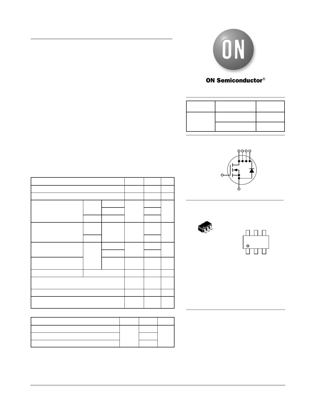
N−Channel
Drain 1 2 5 6
ID Max
5.6 A
4.9 A
Gate 3
Source 4
MARKING DIAGRAM &
PIN ASSIGNMENT
1
TSOP−6
CASE 318G
STYLE 1
Drain Drain Source
654
XX M G
G
123
Drain Drain Gate
XX = Specific Device Code
M = Date Code*
G = Pb−Free Package
(Note: Microdot may be in either location)
*Date Code orientation may vary depending
upon manufacturing location.
ORDERING INFORMATION
See detailed ordering and shipping information ion page 5 of
this data sheet.
© Semiconductor Components Industries, LLC, 2014
August, 2014 − Rev. 1
1
Publication Order Number:
NTGS3130N/D
1 page 
NTGS3130N, NVGS3130N
Table 1. ORDERING INFORMATION
Part Number
Marking
(XX)
Package
Shipping†
NTGS3130NT1G
S9
TSOP−6
3000 / Tape & Reel
(Pb−Free)
NVGS3130NT1G
VS9
TSOP−6
3000 / Tape & Reel
(Pb−Free)
†For information on tape and reel specifications, including part orientation and tape sizes, please refer to our Tape and Reel Packaging
Specifications Brochure, BRD8011/D.
http://onsemi.com
5
5 Page | ||
| Páginas | Total 6 Páginas | |
| PDF Descargar | [ Datasheet NTGS3130N.PDF ] | |
Hoja de datos destacado
| Número de pieza | Descripción | Fabricantes |
| NTGS3130N | Power MOSFET ( Transistor ) | ON Semiconductor |
| Número de pieza | Descripción | Fabricantes |
| SLA6805M | High Voltage 3 phase Motor Driver IC. |
Sanken |
| SDC1742 | 12- and 14-Bit Hybrid Synchro / Resolver-to-Digital Converters. |
Analog Devices |
|
DataSheet.es es una pagina web que funciona como un repositorio de manuales o hoja de datos de muchos de los productos más populares, |
| DataSheet.es | 2020 | Privacy Policy | Contacto | Buscar |