|
|
|
PDF NCP1235 Data sheet ( Hoja de datos )
| Número de pieza | NCP1235 | |
| Descripción | Fixed Frequency Current Mode Controller | |
| Fabricantes | ON Semiconductor | |
| Logotipo | ||
Hay una vista previa y un enlace de descarga de NCP1235 (archivo pdf) en la parte inferior de esta página. Total 30 Páginas | ||
|
No Preview Available !
NCP1235
Product Preview
Fixed Frequency Current
Mode Controller for Flyback
Converters
The NCP1235 is a new fixed−frequency current−mode controller
featuring Dynamic Self−Supply (DSS). This device is pin−to−pin
compatible with the previous NCP12xx families.
The DSS function greatly simplifies the design of the auxiliary
supply and the VCC capacitor by activating the internal startup current
source to supply the controller during transients.
Due to frequency foldback, the controller exhibits excellent
efficiency in light load condition while still achieving very low
standby power consumption. Internal frequency jittering, ramp
compensation, and a versatile latch input make this controller an
excellent candidate for converters where components cost is the key
constraints.
In addition, the controller includes a new high voltage circuitry that
combines a start−up current source and a brown−out detector able to
sense the input voltage either from the rectified ac line or the dc
filtered bulk voltage. The high voltage sensing circuitry is used for the
overpower protection purposes as well. Overpower protection,
overload protection, and next protective features increases safety level
of the final application.
Finally, due to a careful design, the precision of critical parameters
is well controlled over the entire temperature range (−40°C to
+125°C).
www.onsemi.com
MARKING
DIAGRAM
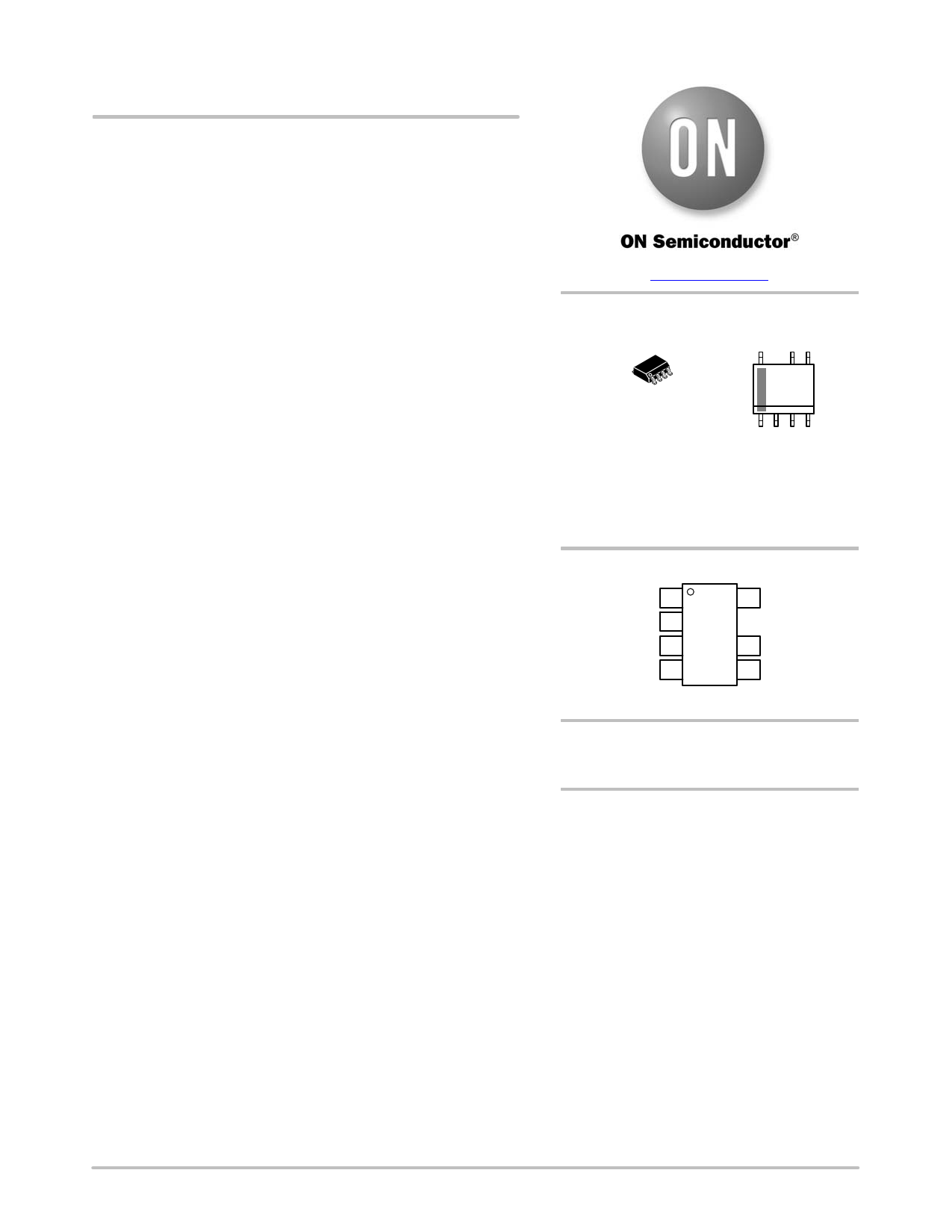
SOIC−7
CASE 751U
8
35A065
ALYWX
G
1
35A065 = Specific Device Code
A = Assembly Location
L = Wafer Lot
Y = Year
W = Work Week
G = Pb−Free Package
PIN CONNECTIONS
Latch 1
FB 2
CS 3
GND 4
8 HV
6 VCC
5 DRV
Features
(Top View)
• Fixed−Frequency Current−Mode Operation with Built−In Ramp
Compensation
• 65 kHz Oscillator Frequency
• Frequency Foldback then Skip Mode for Maximized Performance in
ORDERING INFORMATION
See detailed ordering and shipping information in the package
dimensions section on page 33 of this data sheet.
Light Load and Standby Conditions
• Timer−Based Overload Protection then Device is Latched
• High−voltage Current Source with Brown−Out
• Internal Thermal Shutdown
detection and Dynamic Self−Supply, Simplifying the
Design of the VCC Capacitor
• Frequency Modulation for Softened EMI Signature,
including during Frequency Foldback mode
• Adjustable Overpower Compensation
• Latch−off Input for Severe Fault Conditions, Allowing
Direct Connection of an NTC for Overtemperature
Protection (OTP)
• VCC Operation up to 28 V, with Overvoltage Detection
• $500 mA Peak Source / Sink Current Drive Capability
• Pin−to−Pin Compatible with the Existing NCP12xx
Series
• These Devices are Pb−Free, Halogen Free/BFR Free
and are RoHS Compliant
Typical Applications
• AC−DC Adapters for Notebooks, LCD, and Printers
• Offline Battery Chargers
• Consumer Electronic Power Supplies
• Auxiliary/Housekeeping Power Supplies
• 4.0 ms Soft−Start
This document contains information on a product under development. ON Semiconductor
reserves the right to change or discontinue this product without notice.
© Semiconductor Components Industries, LLC, 2015
January, 2015 − Rev. P0
1
Publication Order Number:
NCP1235/D
1 page 
NCP1235
ELECTRICAL CHARACTERISTICS
(For typical values TJ = 25°C, for min/max values TJ = −40°C to +125°C, VHV = 125 V, VCC = 11 V unless otherwise noted)
Characteristics
Test Condition
Symbol
Min Typ Max
HIGH VOLTAGE CURRENT SOURCE
Minimum voltage for current
source operation
VHV(min)
− 30 60
Current flowing out of VCC pin
VCC = 0 V
VCC = VCC(on) − 0.5 V
Istart1
Istart2
0.2 0.5 0.8
369
Off−state leakage current
SUPPLY
VHV = 500 V
Istart(off)
− 25 50
Turn−on threshold level, VCC
going up
HV current source stop threshold
VCC(on)
11.0 12.0 13.0
HV current source restart threshold
Turn−off threshold
Overvoltage threshold
Blanking duration on VCC(off) and
VCC(ovp) detection (Note 7)
VCC decreasing level at which
the internal logic resets
VCC(min)
VCC(off)
VCC(ovp)
tVCC(blank)
VCC(reset)
9.5 10.5 11.5
8.5 9.5 10.5
25 26.5 28
7 10 13
3.6 5.0 6.0
VCC level for ISTART1 to ISTART2
transition
VCC(inhibit) 0.4 1.0 1.6
Internal current consumption
(Note 6)
BROWN−OUT
DRV open, VFB = 3 V
Cdrv = 1 nF, VFB = 3 V,
Off mode (skip or before start−up)
Fault mode (fault or latch)
ICC1
ICC2
ICC3
ICC4
1.2 1.8 2.2
1.9 2.5 3.2
0.67 0.9 1.13
0.4 0.7 1.0
Brown−Out thresholds
Timer duration for line cycle
drop−out
VHV going up
VHV going down
VHV(start)
VHV(stop)
tHV
92 107 122
79 92 105
47 68 90
OSCILLATOR
Oscillator frequency
fOSC
60 65 70
92 100 108
Maximum duty cycle
Frequency jittering amplitude, in
percentage of FOSC
Frequency jittering modulation
frequency
DMAX
Ajitter
Fjitter
75 80 85
− ±10 −
85 125 165
OUTPUT DRIVER
Rise time, 10% to 90 % of VCC
VCC = VCC(min) + 0.2 V, CDRV = 1 nF
trise − 40 70
Fall time, 90% to 10 % of VCC
VCC = VCC(min) + 0.2 V, CDRV = 1 nF
tfall − 40 70
Current capability
VCC = VCC(min) + 0.2 V, CDRV = 1 nF
DRV high, VDRV = 0 V
DRV low, VDRV = VCC
IDRV(source) − 500 −
IDRV(sink)
− 500 −
Clamping voltage (maximum
gate voltage)
VCC = VCCmax – 0.2 V, DRV high, RDRV
VDRV(clamp)
11
13.5
16
= 33 kW, Cload = 220 pF
High−state voltage drop
VCC = VCC(min) + 0.2 V, RDRV = 33 kW,
VDRV(drop)
−
−
1
DRV high
6. Internal supply current only, current in FB pin not included (current flowing in GND pin only).
7. Guaranteed by design.
Unit
V
mA
mA
V
V
V
V
ms
V
V
mA
V
ms
kHz
%
%
Hz
ns
ns
mA
V
V
www.onsemi.com
5
5 Page 
NCP1235
TYPICAL PERFORMANCE CHARACTERISTICS
150
145
140
135
130
125
120
115
110
−50 −25
0
25 50 75 100 125
TEMPERATURE (°C)
Figure 20. Maximum Overpower
Compensating Current IOPC(365) Flowing Out
of CS Pin
2.40
2.35
2.30
2.25
2.20
2.15
2.10
2.05
2.00
1.95
1.90
−50 −25
0 25 50 75
TEMPERATURE (°C)
100 125
Figure 22. FB Pin Level VFB(OPCE) Below
Which is No Overpower Compensation
Applied
2.60
2.55
2.50
2.45
2.40
2.35
2.30
2.25
2.20
2.15
2.10
−50 −25
0 25 50 75
TEMPERATURE (°C)
100
Figure 21. FB Pin Level VFB(OPCF) Above
Which is the Overpower Compensation
Applied
2.65
125
2.60
2.55
2.50
2.45
2.40
2.35
−50 −25
0 25 50 75
TEMPERATURE (°C)
100 125
Figure 23. Latch Pin High Threshold VOVP
0.85
0.84
0.83
0.82
0.81
0.80
0.79
0.78
0.77
0.76
0.75
−50 −25
0 25 50 75
TEMPERATURE (°C)
100
Figure 24. Latch Pin Low Threshold VOTP
125
1.34
1.32
1.30
1.28
1.26
1.24
1.22
1.20
1.18
−50
−25
0
25 50 75 100
TEMPERATURE (°C)
Figure 25. Latch Pin Open Voltage Vclamp0
125
www.onsemi.com
11
11 Page | ||
| Páginas | Total 30 Páginas | |
| PDF Descargar | [ Datasheet NCP1235.PDF ] | |
Hoja de datos destacado
| Número de pieza | Descripción | Fabricantes |
| NCP1230 | Low Standby Power High Performance PWM Controller | ON Semiconductor |
| NCP1230A | Low-Standby Power Soft Skip Mode Controller | ON Semiconductor |
| NCP1231 | Low Standby Power High Performance PWM Controller | ON Semiconductor |
| NCP1232 | Microprocessor Monitor | ON |
| Número de pieza | Descripción | Fabricantes |
| SLA6805M | High Voltage 3 phase Motor Driver IC. |
Sanken |
| SDC1742 | 12- and 14-Bit Hybrid Synchro / Resolver-to-Digital Converters. |
Analog Devices |
|
DataSheet.es es una pagina web que funciona como un repositorio de manuales o hoja de datos de muchos de los productos más populares, |
| DataSheet.es | 2020 | Privacy Policy | Contacto | Buscar |