|
|
|
PDF NTLLD4951NF Data sheet ( Hoja de datos )
| Número de pieza | NTLLD4951NF | |
| Descripción | Dual N-Channel Power MOSFET | |
| Fabricantes | ON Semiconductor | |
| Logotipo | ||
Hay una vista previa y un enlace de descarga de NTLLD4951NF (archivo pdf) en la parte inferior de esta página. Total 12 Páginas | ||
|
No Preview Available !
NTLLD4951NF
Dual N-Channel Power
MOSFET with Integrated
Schottky
30 V, High Side 11 A / Low Side 13 A,
Dual N−Channel, WDFN (3 mm x 3 mm)
Features
• Co−Packaged Power Stage Solution to Minimize Board Space
• Low Side MOSFET with Integrated Schottky
• Minimized Parasitic Inductances
• Optimized Devices to Reduce Power Losses
• These Devices are Pb−Free, Halogen Free/BFR Free and are RoHS
Compliant
Applications
• DC−DC Converters
• System Voltage Rails
• Point of Load
http://onsemi.com
V(BR)DSS
Q1 Top FET
30 V
Q2 Bottom
FET 30 V
RDS(ON) MAX
17.4 mW @ 10 V
25 mW @ 4.5 V
13.3 mW @ 10 V
20 mW @ 4.5 V
ID MAX
11 A
13 A
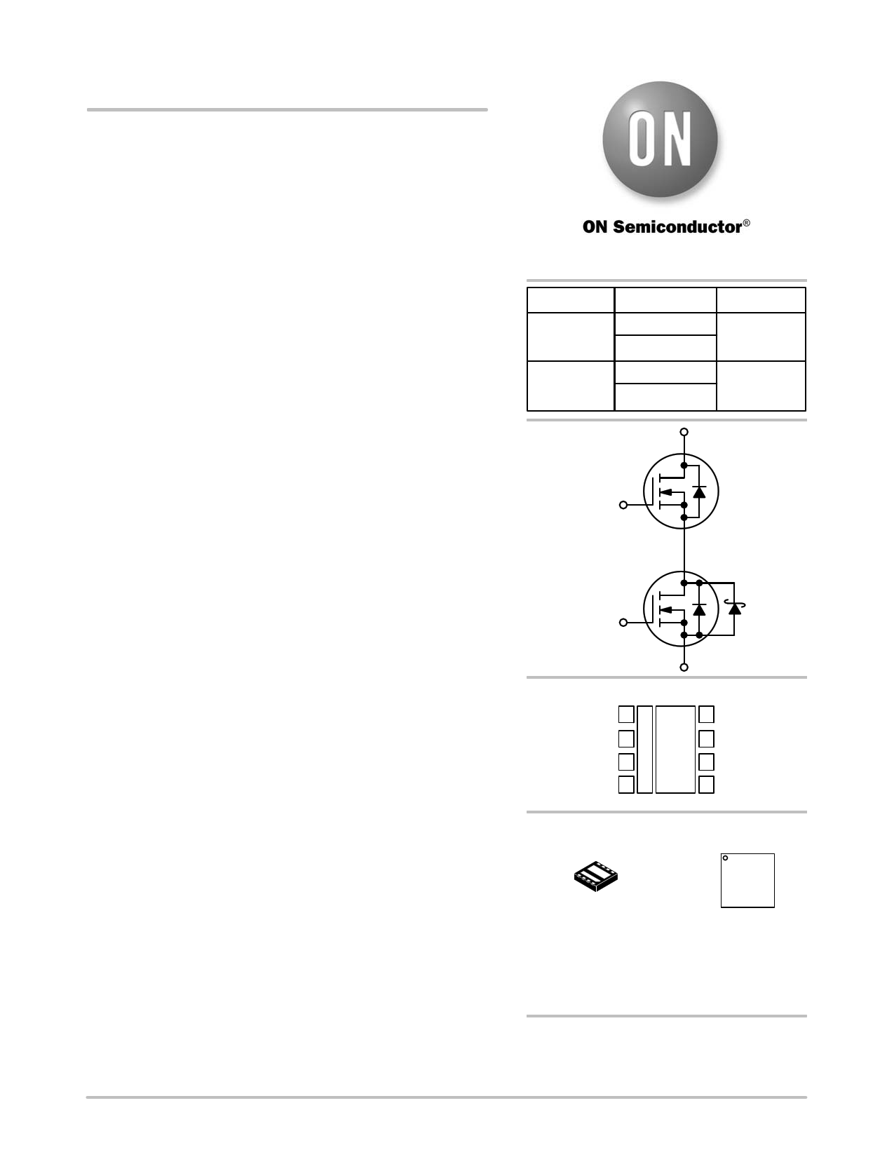
D1 (2, 3, 4, 9)
(1) G1
S1/D2 (10)
© Semiconductor Components Industries, LLC, 2013
October, 2013 − Rev. 0
(8) G2
S2 (5, 6, 7)
PIN CONNECTIONS
D1 4
5 S2
D1 3 9 10 6 S2
D1 2 D1 S1/D2 7 S2
G1 1
8 G2
(Bottom View)
MARKING
DIAGRAM
1
WDFN8
4951
1
CASE 511BP
AYWWG
G
4951
A
Y
WW
G
= Specific Device Code
= Assembly Location
= Year
= Work Week
= Pb−Free Package
(Note: Microdot may be in either location)
ORDERING INFORMATION
See detailed ordering and shipping information in the package
dimensions section on page 5 of this data sheet.
1 Publication Order Number:
NTLLD4951NF/D
1 page 
NTLLD4951NF
ELECTRICAL CHARACTERISTICS (TJ = 25°C unless otherwise specified)
Parameter
FET Symbol
Test Condition
DRAIN−SOURCE DIODE CHARACTERISTICS
Reverse Recovery Time
Q1
Q2 tRR
Charge Time
Discharge Time
Q1
ta
Q2
Q1
tb
Q2
VGS = 0 V, dIS/dt = 100 A/ms, IS = 3 A
Reverse Recovery Charge
Q1
Q2
QRR
PACKAGE PARASITIC VALUES
Source Inductance
Q1
Q2 LS
Drain Inductance
Gate Inductance
Q1
Q2 LD
Q1
Q2 LG
TA = 25°C
Gate Resistance
Q1
Q2 RG
5. Pulse Test: pulse width ≤ 300 ms, duty cycle ≤ 2%
6. Switching characteristics are independent of operating junction temperatures.
Min Typ Max Unit
17.9
23.3
9.0
ns
11.3
9.0
12
8.0
12 nC
0.36
0.36
0.054
0.054
1.3
1.3
0.8
0.8
nH
nH
nH
W
ORDERING INFORMATION
Device
Package
Shipping†
NTLLD4951NFTWG
WDFN8
(Pb−Free)
3000 / Tape & Reel
†For information on tape and reel specifications, including part orientation and tape sizes, please refer to our Tape and Reel Packaging
Specifications Brochure, BRD8011/D.
http://onsemi.com
5
5 Page 
NTLLD4951NF
TYPICAL CHARACTERISTICS − Q2
100
D = 0.5
0.2
10 0.1
0.05
0.02
1 0.01
0.1
SINGLE PULSE
0.01
0.000001 0.00001
0.0001
0.001
0.01
0.1
t, PULSE TIME (sec)
Figure 26. Thermal Response
1
10 100 1000
http://onsemi.com
11
11 Page | ||
| Páginas | Total 12 Páginas | |
| PDF Descargar | [ Datasheet NTLLD4951NF.PDF ] | |
Hoja de datos destacado
| Número de pieza | Descripción | Fabricantes |
| NTLLD4951NF | Dual N-Channel Power MOSFET | ON Semiconductor |
| Número de pieza | Descripción | Fabricantes |
| SLA6805M | High Voltage 3 phase Motor Driver IC. |
Sanken |
| SDC1742 | 12- and 14-Bit Hybrid Synchro / Resolver-to-Digital Converters. |
Analog Devices |
|
DataSheet.es es una pagina web que funciona como un repositorio de manuales o hoja de datos de muchos de los productos más populares, |
| DataSheet.es | 2020 | Privacy Policy | Contacto | Buscar |