|
|
|
PDF NTNS4C69N Data sheet ( Hoja de datos )
| Número de pieza | NTNS4C69N | |
| Descripción | Small Signal MOSFET | |
| Fabricantes | ON Semiconductor | |
| Logotipo | ||
Hay una vista previa y un enlace de descarga de NTNS4C69N (archivo pdf) en la parte inferior de esta página. Total 5 Páginas | ||
|
No Preview Available !
NTNS4C69N
Small Signal MOSFET
30 V, 820 mA, Single N−Channel SOT−883
(XDFN3) 1.0 x 0.6 x 0.4 mm Package
Features
• Single N−Channel MOSFET
• Ultra Low Profile SOT−883 (XDFN3) 1.0 x 0.6 x 0.4 mm for
Extremely Thin Environments such as Portable Electronics
• Low RDS(on) Solution in Ultra Small 1.0 x 0.6 mm Package
• 1.8 V Gate Drive
• These Devices are Pb−Free, Halogen Free/BFR Free and are RoHS
Compliant
Applications
• High Side Switch
• High Speed Interfacing
• Level Shift and Translate
• Optimized for DC−DC Converter Power Management in Ultra
Portable Solutions
MAXIMUM RATINGS (TJ = 25°C unless otherwise stated)
Parameter
Symbol Value
Units
Drain-to-Source Voltage
Gate-to-Source Voltage
Continuous Drain Steady
Current (Note 1)
State
Power Dissipa-
tion (Note 1)
t≤5s
Steady
State
TA = 25°C
TA = 85°C
TA = 25°C
TA = 25°C
VDSS
VGS
ID
PD
30 V
±12 V
820 mA
590
970
156 mW
t ≤ 5 s TA = 25°C
Pulsed Drain Current
tp = 10 ms
Operating Junction and Storage
Temperature
Source Current (Body Diode) (Note 2)
Lead Temperature for Soldering Purposes
(1/8″ from case for 10 s)
IDM
TJ,
TSTG
IS
TL
220
2.4
-55 to
150
156
260
mA
°C
mA
°C
Stresses exceeding those listed in the Maximum Ratings table may damage the
device. If any of these limits are exceeded, device functionality should not be
assumed, damage may occur and reliability may be affected.
THERMAL RESISTANCE RATINGS
Parameter
Symbol Max Units
Junction-to-Ambient – Steady State (Note 1)
RθJA
800 °C/W
Junction-to-Ambient – t ≤ 5 s (Note 1)
RθJA
570
1. Surface Mounted on FR4 Board using the minimum recommended pad size,
(or 2 mm2), 1 oz Cu.
2. Pulse Test: pulse width ≤ 300 ms, duty cycle ≤ 2%.
www.onsemi.com
V(BR)DSS
30 V
MOSFET
RDS(on) MAX
0.155 W @ 4.5 V
0.168 W @ 3.7 V
0.180 W @ 3.3 V
0.220 W @ 2.5 V
0.450 W @ 1.8 V
ID MAX
820 mA
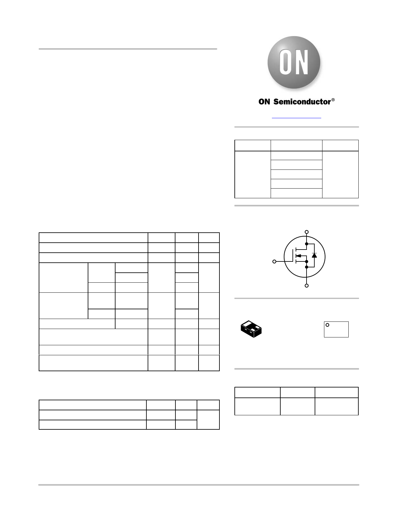
N−Channel MOSFET
D (3)
G (1)
S (2)
3
21
SOT−883
(XDFN3)
CASE 506CB
MARKING
DIAGRAM
AA M
AA = Specific Device Code
M = Date Code
ORDERING INFORMATION
Device
Package
Shipping†
NTNS4C69NTCG SOT−883
(Pb−Free)
8000 /
Tape & Reel
†For information on tape and reel specifications,
including part orientation and tape sizes, please
refer to our Tape and Reel Packaging Specifications
Brochure, BRD8011/D.
© Semiconductor Components Industries, LLC, 2016
January, 2016 − Rev. 0
1
Publication Order Number:
NTNS4C69N/D
1 page 
NTNS4C69N
PACKAGE DIMENSIONS
SOT−883 (XDFN3), 1.0x0.6, 0.35P
CASE 506CB
ISSUE A
PIN ONE
ÉÉÉÉÉÉREFERENCE
D
0.10 C
AB
E
0.10 C
0.10 C
TOP VIEW
NOTE 3
A
3X 0.10 C
A1
SIDE VIEW
D2
C
SEATING
PLANE
e/2
0.10 M
0.05 M
e
2X b
CA B
C
E2
1
3X L
BOTTOM VIEW
NOTES:
1. DIMENSIONING AND TOLERANCING PER
ASME Y14.5M, 1994.
2. CONTROLLING DIMENSION: MILLIMETERS.
3. EXPOSED COPPER ALLOWED AS SHOWN.
MILLIMETERS
DIM MIN MAX
A 0.340 0.440
A1 0.000 0.030
b 0.075 0.200
D 0.950 1.075
D2 0.620 BSC
e 0.350 BSC
E 0.550 0.675
E2 0.425 0.550
L 0.170 0.300
RECOMMENDED
SOLDER FOOTPRINT*
1.10
2X 0.43
1
0.41
0.55
2X 0.20
PACKAGE
OUTLINE
DIMENSIONS: MILLIMETERS
*For additional information on our Pb−Free strategy and soldering
details, please download the ON Semiconductor Soldering and
Mounting Techniques Reference Manual, SOLDERRM/D.
ON Semiconductor and the
are registered trademarks of Semiconductor Components Industries, LLC (SCILLC) or its subsidiaries in the United States and/or other countries.
SCILLC owns the rights to a number of patents, trademarks, copyrights, trade secrets, and other intellectual property. A listing of SCILLC’s product/patent coverage may be accessed
at www.onsemi.com/site/pdf/Patent−Marking.pdf. SCILLC reserves the right to make changes without further notice to any products herein. SCILLC makes no warranty, representation
or guarantee regarding the suitability of its products for any particular purpose, nor does SCILLC assume any liability arising out of the application or use of any product or circuit, and
specifically disclaims any and all liability, including without limitation special, consequential or incidental damages. “Typical” parameters which may be provided in SCILLC data sheets
and/or specifications can and do vary in different applications and actual performance may vary over time. All operating parameters, including “Typicals” must be validated for each
customer application by customer’s technical experts. SCILLC does not convey any license under its patent rights nor the rights of others. SCILLC products are not designed, intended,
or authorized for use as components in systems intended for surgical implant into the body, or other applications intended to support or sustain life, or for any other application in which
the failure of the SCILLC product could create a situation where personal injury or death may occur. Should Buyer purchase or use SCILLC products for any such unintended or
unauthorized application, Buyer shall indemnify and hold SCILLC and its officers, employees, subsidiaries, affiliates, and distributors harmless against all claims, costs, damages, and
expenses, and reasonable attorney fees arising out of, directly or indirectly, any claim of personal injury or death associated with such unintended or unauthorized use, even if such claim
alleges that SCILLC was negligent regarding the design or manufacture of the part. SCILLC is an Equal Opportunity/Affirmative Action Employer. This literature is subject to all applicable
copyright laws and is not for resale in any manner.
PUBLICATION ORDERING INFORMATION
LITERATURE FULFILLMENT:
Literature Distribution Center for ON Semiconductor
19521 E. 32nd Pkwy, Aurora, Colorado 80011 USA
Phone: 303−675−2175 or 800−344−3860 Toll Free USA/Canada
Fax: 303−675−2176 or 800−344−3867 Toll Free USA/Canada
Email: [email protected]
N. American Technical Support: 800−282−9855 Toll Free
USA/Canada
Europe, Middle East and Africa Technical Support:
Phone: 421 33 790 2910
Japan Customer Focus Center
Phone: 81−3−5817−1050
ON Semiconductor Website: www.onsemi.com
Order Literature: http://www.onsemi.com/orderlit
For additional information, please contact your local
Sales Representative
www.onsemi.com
5
NTNS4C69N/D
5 Page | ||
| Páginas | Total 5 Páginas | |
| PDF Descargar | [ Datasheet NTNS4C69N.PDF ] | |
Hoja de datos destacado
| Número de pieza | Descripción | Fabricantes |
| NTNS4C69N | Small Signal MOSFET | ON Semiconductor |
| Número de pieza | Descripción | Fabricantes |
| SLA6805M | High Voltage 3 phase Motor Driver IC. |
Sanken |
| SDC1742 | 12- and 14-Bit Hybrid Synchro / Resolver-to-Digital Converters. |
Analog Devices |
|
DataSheet.es es una pagina web que funciona como un repositorio de manuales o hoja de datos de muchos de los productos más populares, |
| DataSheet.es | 2020 | Privacy Policy | Contacto | Buscar |