|
|
|
PDF NSBA144TF3 Data sheet ( Hoja de datos )
| Número de pieza | NSBA144TF3 | |
| Descripción | Digital Transistors | |
| Fabricantes | ON Semiconductor | |
| Logotipo | ||
Hay una vista previa y un enlace de descarga de NSBA144TF3 (archivo pdf) en la parte inferior de esta página. Total 11 Páginas | ||
|
No Preview Available !
MUN2140, MMUN2140L,
MUN5140, DTA114TE,
DTA144TM3, NSBA144TF3
Digital Transistors (BRT)
R1 = 47 kW, R2 = 8 kW
PNP Transistors with Monolithic Bias
Resistor Network
This series of digital transistors is designed to replace a single
device and its external resistor bias network. The Bias Resistor
Transistor (BRT) contains a single transistor with a monolithic bias
network consisting of two resistors; a series base resistor and a base−
emitter resistor. The BRT eliminates these individual components by
integrating them into a single device. The use of a BRT can reduce
both system cost and board space.
Features
• Simplifies Circuit Design
• Reduces Board Space
• Reduces Component Count
• S and NSV Prefix for Automotive and Other Applications Requiring
Unique Site and Control Change Requirements; AEC-Q101 Qualified
and PPAP Capable
• These Devices are Pb−Free, Halogen Free/BFR Free and are RoHS
Compliant
MAXIMUM RATINGS (TA = 25°C)
Rating
Symbol
Max
Unit
Collector−Base Voltage
VCBO
50
Vdc
Collector−Emitter Voltage
VCEO
50
Vdc
Collector Current − Continuous
IC 100 mAdc
Input Forward Voltage
VIN(fwd)
40
Vdc
Input Reverse Voltage
VIN(rev)
5
Vdc
Stresses exceeding Maximum Ratings may damage the device. Maximum
Ratings are stress ratings only. Functional operation above the Recommended
Operating Conditions is not implied. Extended exposure to stresses above the
Recommended Operating Conditions may affect device reliability.
http://onsemi.com
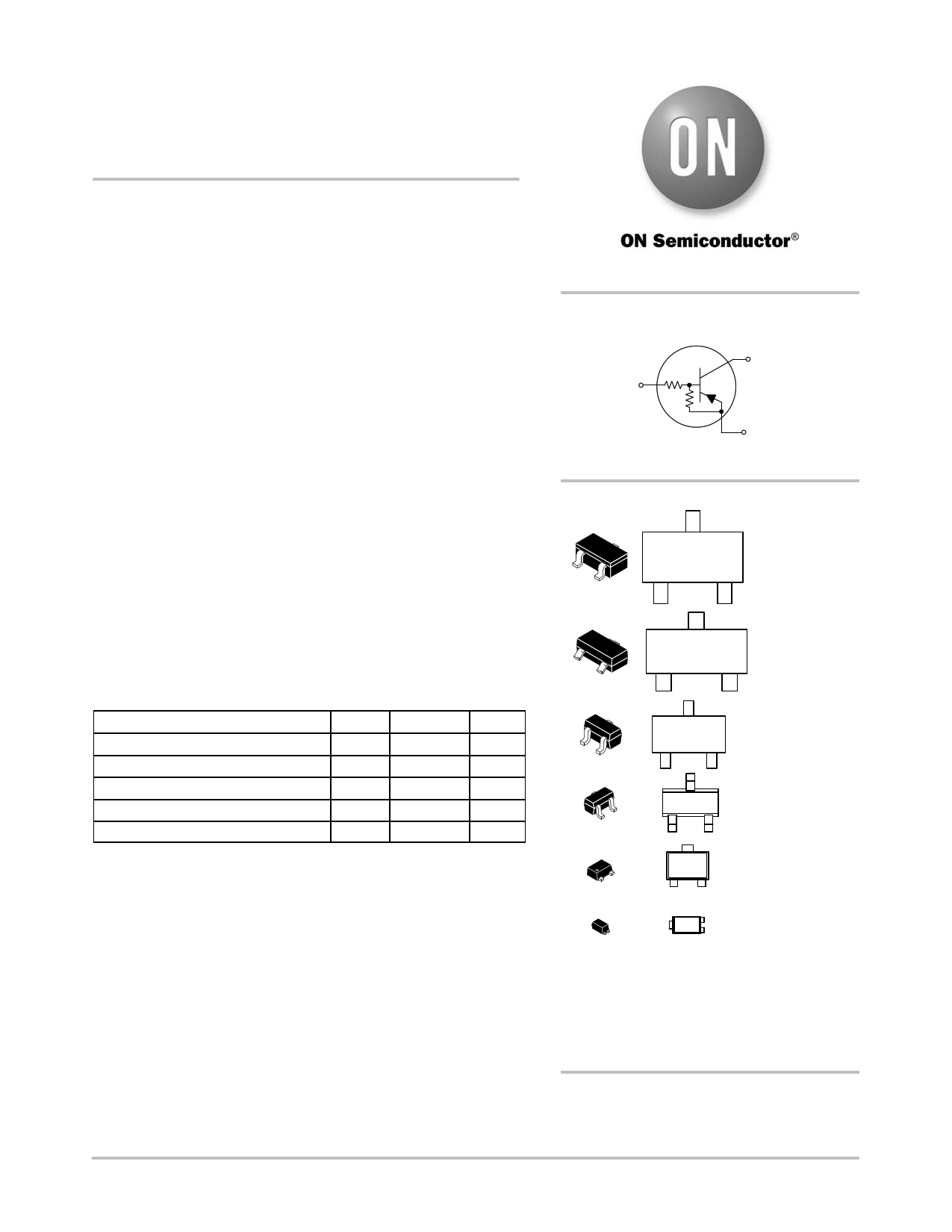
PIN CONNECTIONS
PIN 3
COLLECTOR
PIN 1
BASE
R1
(OUTPUT)
(INPUT) R2
PIN 2
EMITTER
(GROUND)
MARKING DIAGRAMS
XX MG
G
1
SC−59
CASE 318D
STYLE 1
XXX MG
G
1
SOT−23
CASE 318
STYLE 6
XX MG
G
1
XX M
1
SC−70/SOT−323
CASE 419
STYLE 3
SC−75
CASE 463
STYLE 1
XX M
1
XM 1
SOT−723
CASE 631AA
STYLE 1
SOT−1123
CASE 524AA
STYLE 1
XXX
M
G
= Specific Device Code
= Date Code*
= Pb−Free Package
(Note: Microdot may be in either location)
*Date Code orientation may vary depending
upon manufacturing location.
© Semiconductor Components Industries, LLC, 2013
February, 2013 − Rev. 2
ORDERING INFORMATION
See detailed ordering, marking, and shipping information in
the package dimensions section on page 2 of this data sheet.
1 Publication Order Number:
DTA144T/D
1 page 
MUN2140, MMUN2140L, MUN5140, DTA114TE, DTA144TM3, NSBA144TF3
10
IC/IB = 10
1
25°C
0.1 150°C
TYPICAL CHARACTERISTICS
MUN2140, MMUN2140L, MUN5140, DTA144TE, DTA144TM3
1000
150°C
25°C
100 −55°C
10
−55°C
0.01
0
10 20 30 40
IC, COLLECTOR CURRENT (mA)
Figure 2. VCE(sat) vs. IC
1
50 1
VCE = 10 V
10
IC, COLLECTOR CURRENT (mA)
Figure 3. DC Current Gain
100
10 100
9
f = 10 kHz
IE = 0 A
150°C
−55°C
8
TA = 25°C
10
7 25°C
61
5
4 0.1
3
2 0.01
1 VO = 5 V
0 0.001
0 10 20 30 40 50
0 4 8 12 16 20 24 28
VR, REVERSE VOLTAGE (V)
Vin, INPUT VOLTAGE (V)
Figure 4. Output Capacitance
Figure 5. Output Current vs. Input Voltage
100
25°C
10
−55°C
1
150°C
0.1
0
VO = 0.2 V
10 20 30 40
IC, COLLECTOR CURRENT (mA)
Figure 6. Input Voltage vs. Output Current
50
http://onsemi.com
5
5 Page 
MUN2140, MMUN2140L, MUN5140, DTA114TE, DTA144TM3, NSBA144TF3
PACKAGE DIMENSIONS
D −X−
−Y−
1 3E
2
TOP VIEW
A
SOT−1123
CASE 524AA
ISSUE C
c HE
SIDE VIEW
3X L2
e
b
0.08 X Y
2X b1
3X L
BOTTOM VIEW
NOTES:
1. DIMENSIONING AND TOLERANCING PER ASME
Y14.5M, 1994.
2. CONTROLLING DIMENSION: MILLIMETERS.
3. MAXIMUM LEAD THICKNESS INCLUDES LEAD
FINISH. MINIMUM LEAD THICKNESS IS THE
MINIMUM THICKNESS OF BASE MATERIAL.
4. DIMENSIONS D AND E DO NOT INCLUDE MOLD
FLASH, PROTRUSIONS, OR GATE BURRS.
MILLIMETERS
DIM MIN MAX
A 0.34 0.40
b 0.15 0.28
b1 0.10 0.20
c 0.07 0.17
D 0.75 0.85
E 0.55 0.65
e 0.35 0.40
HE 0.95 1.05
L 0.185 REF
L2 0.05 0.15
STYLE 1:
PIN 1. BASE
2. EMITTER
3. COLLECTOR
SOLDERING FOOTPRINT*
1.20
3X 0.34
1
0.26
0.38 2X
0.20
PACKAGE
OUTLINE
DIMENSIONS: MILLIMETERS
*For additional information on our Pb−Free strategy and soldering
details, please download the ON Semiconductor Soldering and
Mounting Techniques Reference Manual, SOLDERRM/D.
ON Semiconductor and
are registered trademarks of Semiconductor Components Industries, LLC (SCILLC). SCILLC owns the rights to a number of patents, trademarks,
copyrights, trade secrets, and other intellectual property. A listing of SCILLC’s product/patent coverage may be accessed at www.onsemi.com/site/pdf/Patent−Marking.pdf. SCILLC
reserves the right to make changes without further notice to any products herein. SCILLC makes no warranty, representation or guarantee regarding the suitability of its products for any
particular purpose, nor does SCILLC assume any liability arising out of the application or use of any product or circuit, and specifically disclaims any and all liability, including without
limitation special, consequential or incidental damages. “Typical” parameters which may be provided in SCILLC data sheets and/or specifications can and do vary in different applications
and actual performance may vary over time. All operating parameters, including “Typicals” must be validated for each customer application by customer’s technical experts. SCILLC
does not convey any license under its patent rights nor the rights of others. SCILLC products are not designed, intended, or authorized for use as components in systems intended for
surgical implant into the body, or other applications intended to support or sustain life, or for any other application in which the failure of the SCILLC product could create a situation where
personal injury or death may occur. Should Buyer purchase or use SCILLC products for any such unintended or unauthorized application, Buyer shall indemnify and hold SCILLC and
its officers, employees, subsidiaries, affiliates, and distributors harmless against all claims, costs, damages, and expenses, and reasonable attorney fees arising out of, directly or indirectly,
any claim of personal injury or death associated with such unintended or unauthorized use, even if such claim alleges that SCILLC was negligent regarding the design or manufacture
of the part. SCILLC is an Equal Opportunity/Affirmative Action Employer. This literature is subject to all applicable copyright laws and is not for resale in any manner.
PUBLICATION ORDERING INFORMATION
LITERATURE FULFILLMENT:
Literature Distribution Center for ON Semiconductor
P.O. Box 5163, Denver, Colorado 80217 USA
Phone: 303−675−2175 or 800−344−3860 Toll Free USA/Canada
Fax: 303−675−2176 or 800−344−3867 Toll Free USA/Canada
Email: [email protected]
N. American Technical Support: 800−282−9855 Toll Free
USA/Canada
Europe, Middle East and Africa Technical Support:
Phone: 421 33 790 2910
Japan Customer Focus Center
Phone: 81−3−5817−1050
http://onsemi.com
11
ON Semiconductor Website: www.onsemi.com
Order Literature: http://www.onsemi.com/orderlit
For additional information, please contact your local
Sales Representative
DTA144T/D
11 Page | ||
| Páginas | Total 11 Páginas | |
| PDF Descargar | [ Datasheet NSBA144TF3.PDF ] | |
Hoja de datos destacado
| Número de pieza | Descripción | Fabricantes |
| NSBA144TF3 | Digital Transistors | ON Semiconductor |
| Número de pieza | Descripción | Fabricantes |
| SLA6805M | High Voltage 3 phase Motor Driver IC. |
Sanken |
| SDC1742 | 12- and 14-Bit Hybrid Synchro / Resolver-to-Digital Converters. |
Analog Devices |
|
DataSheet.es es una pagina web que funciona como un repositorio de manuales o hoja de datos de muchos de los productos más populares, |
| DataSheet.es | 2020 | Privacy Policy | Contacto | Buscar |