|
|
|
PDF NSBC113EF3 Data sheet ( Hoja de datos )
| Número de pieza | NSBC113EF3 | |
| Descripción | Digital Transistors | |
| Fabricantes | ON Semiconductor | |
| Logotipo | ||
Hay una vista previa y un enlace de descarga de NSBC113EF3 (archivo pdf) en la parte inferior de esta página. Total 12 Páginas | ||
|
No Preview Available !
MUN2230, MMUN2230L,
MUN5230, DTC113EE,
DTC113EM3, NSBC113EF3
Digital Transistors (BRT)
R1 = 1 kW, R2 = 1 kW
NPN Transistors with Monolithic Bias
Resistor Network
This series of digital transistors is designed to replace a single
device and its external resistor bias network. The Bias Resistor
Transistor (BRT) contains a single transistor with a monolithic bias
network consisting of two resistors; a series base resistor and a base−
emitter resistor. The BRT eliminates these individual components by
integrating them into a single device. The use of a BRT can reduce
both system cost and board space.
Features
• Simplifies Circuit Design
• Reduces Board Space
• Reduces Component Count
• S and NSV Prefix for Automotive and Other Applications Requiring
Unique Site and Control Change Requirements; AEC-Q101 Qualified
and PPAP Capable
• These Devices are Pb−Free, Halogen Free/BFR Free and are RoHS
Compliant
MAXIMUM RATINGS (TA = 25°C)
Rating
Symbol
Max
Unit
Collector−Base Voltage
VCBO
50
Vdc
Collector−Emitter Voltage
VCEO
50
Vdc
Collector Current − Continuous
IC 100 mAdc
Input Forward Voltage
VIN(fwd)
10
Vdc
Input Reverse Voltage
VIN(rev)
10
Vdc
Stresses exceeding those listed in the Maximum Ratings table may damage the
device. If any of these limits are exceeded, device functionality should not be
assumed, damage may occur and reliability may be affected.
www.onsemi.com
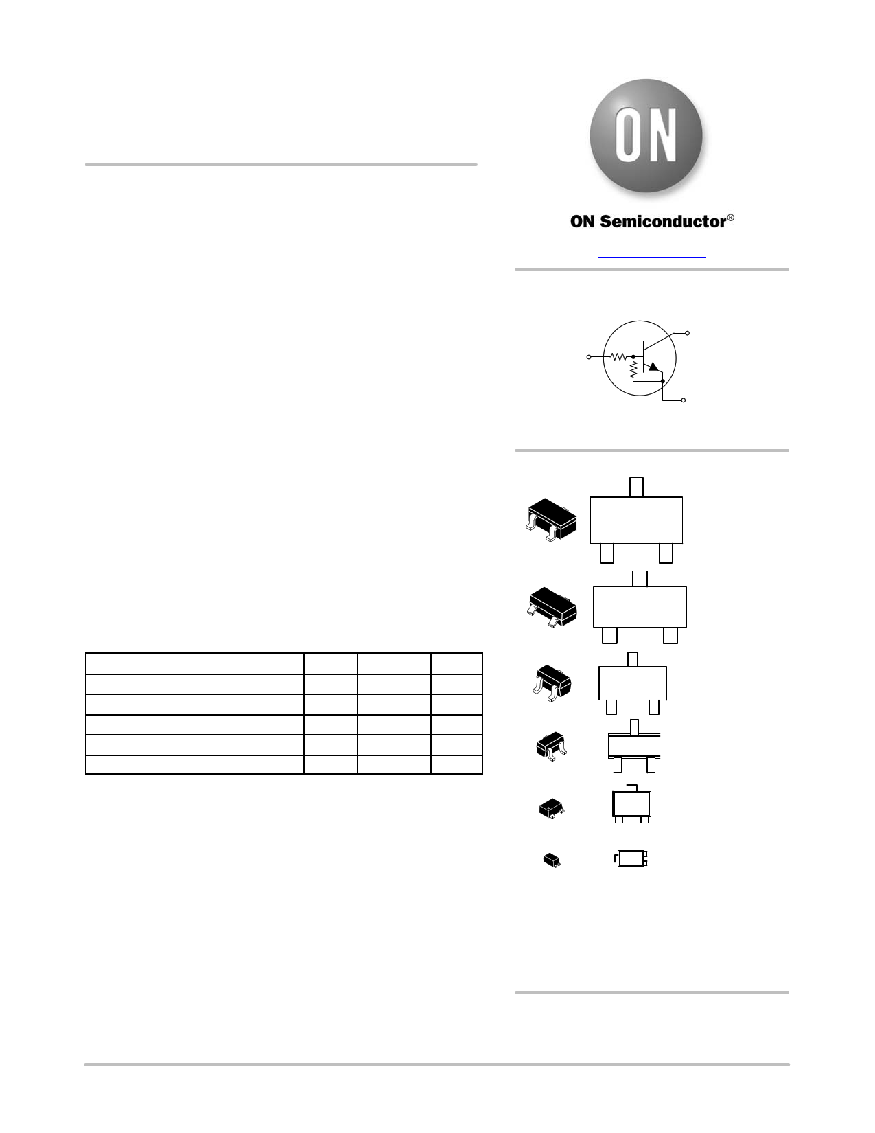
PIN CONNECTIONS
PIN 1
BASE
(INPUT)
R1
R2
PIN 3
COLLECTOR
(OUTPUT)
PIN 2
EMITTER
(GROUND)
MARKING DIAGRAMS
XX MG
G
1
SC−59
CASE 318D
STYLE 1
XXX MG
G
1
SOT−23
CASE 318
STYLE 6
XX MG
G
1
XX M
1
SC−70/SOT−323
CASE 419
STYLE 3
SC−75
CASE 463
STYLE 1
XX M
1
XM 1
SOT−723
CASE 631AA
STYLE 1
SOT−1123
CASE 524AA
STYLE 1
XXX
M
G
= Specific Device Code
= Date Code*
= Pb−Free Package
(Note: Microdot may be in either location)
*Date Code orientation may vary depending up-
on manufacturing location.
ORDERING INFORMATION
See detailed ordering, marking, and shipping information in
the package dimensions section on page 2 of this data sheet.
© Semiconductor Components Industries, LLC, 2015
January, 2015 − Rev. 3
1
Publication Order Number:
DTC113E/D
1 page 
MUN2230, MMUN2230L, MUN5230, DTC113EE, DTC113EM3, NSBC113EF3
Table 3. ELECTRICAL CHARACTERISTICS (TA = 25°C, unless otherwise noted)
Characteristic
Symbol Min Typ Max
Unit
OFF CHARACTERISTICS
Collector−Base Cutoff Current
(VCB = 50 V, IE = 0)
ICBO
nAdc
− − 100
Collector−Emitter Cutoff Current
(VCE = 50 V, IB = 0)
ICEO
nAdc
− − 500
Emitter−Base Cutoff Current
(VEB = 6.0 V, IC = 0)
IEBO
mAdc
− − 4.3
Collector−Base Breakdown Voltage
(IC = 10 mA, IE = 0)
V(BR)CBO
50
−
−
Vdc
Collector−Emitter Breakdown Voltage (Note 5)
(IC = 2.0 mA, IB = 0)
V(BR)CEO
50
−
−
Vdc
ON CHARACTERISTICS
DC Current Gain (Note 5)
(IC = 5.0 mA, VCE = 10 V)
hFE
3.0 5.0
−
Collector−Emitter Saturation Voltage (Note 5)
(IC = 10 mA, IB = 5.0 mA)
VCE(sat)
−
− 0.25
Vdc
Input Voltage (off)
(VCE = 5.0 V, IC = 100 mA)
Vi(off)
− 1.2 0.5
Vdc
Input Voltage (on)
(VCE = 0.3 V, IC = 20 mA)
Vi(on)
2 1.6 −
Vdc
Output Voltage (on)
(VCC = 5.0 V, VB = 2.5 V, RL = 1.0 kW)
Output Voltage (off)
(VCC = 5.0 V, VB = 0.05 V, RL = 1.0 kW)
VOL Vdc
− − 0.2
VOH
4.9 −
−
Vdc
Input Resistor
R1
0.7 1.0 1.3
kW
Resistor Ratio
R1/R2
0.8 1.0 1.2
Product parametric performance is indicated in the Electrical Characteristics for the listed test conditions, unless otherwise noted. Product
performance may not be indicated by the Electrical Characteristics if operated under different conditions.
5. Pulsed Condition: Pulse Width = 300 msec, Duty Cycle ≤ 2%.
www.onsemi.com
5
5 Page 
MUN2230, MMUN2230L, MUN5230, DTC113EE, DTC113EM3, NSBC113EF3
PACKAGE DIMENSIONS
−X−
D
b1
3
−Y−
E
2X e
12
2X b
0.08 X Y
TOP VIEW
3X L
1
3X L2
BOTTOM VIEW
SOT−723
CASE 631AA
ISSUE D
A
HE
C
SIDE VIEW
NOTES:
1. DIMENSIONING AND TOLERANCING PER ASME
Y14.5M, 1994.
2. CONTROLLING DIMENSION: MILLIMETERS.
3. MAXIMUM LEAD THICKNESS INCLUDES LEAD
FINISH. MINIMUM LEAD THICKNESS IS THE MINIMUM
THICKNESS OF BASE MATERIAL.
4. DIMENSIONS D AND E DO NOT INCLUDE MOLD
FLASH, PROTRUSIONS OR GATE BURRS.
MILLIMETERS
DIM MIN NOM MAX
A 0.45 0.50 0.55
b 0.15 0.21 0.27
b1 0.25 0.31 0.37
C 0.07 0.12 0.17
D 1.15 1.20 1.25
E 0.75 0.80 0.85
e 0.40 BSC
H E 1.15 1.20 1.25
L 0.29 REF
L2 0.15 0.20 0.25
STYLE 1:
PIN 1. BASE
2. EMITTER
3. COLLECTOR
RECOMMENDED
SOLDERING FOOTPRINT*
2X 0.27
2X
0.40
PACKAGE
OUTLINE
1.50
3X 0.52
0.36
DIMENSIONS: MILLIMETERS
*For additional information on our Pb−Free strategy and soldering
details, please download the ON Semiconductor Soldering and
Mounting Techniques Reference Manual, SOLDERRM/D.
www.onsemi.com
11
11 Page | ||
| Páginas | Total 12 Páginas | |
| PDF Descargar | [ Datasheet NSBC113EF3.PDF ] | |
Hoja de datos destacado
| Número de pieza | Descripción | Fabricantes |
| NSBC113EF3 | Digital Transistors | ON Semiconductor |
| Número de pieza | Descripción | Fabricantes |
| SLA6805M | High Voltage 3 phase Motor Driver IC. |
Sanken |
| SDC1742 | 12- and 14-Bit Hybrid Synchro / Resolver-to-Digital Converters. |
Analog Devices |
|
DataSheet.es es una pagina web que funciona como un repositorio de manuales o hoja de datos de muchos de los productos más populares, |
| DataSheet.es | 2020 | Privacy Policy | Contacto | Buscar |