|
|
PDF NCN5151 Data sheet ( Hoja de datos )
| Número de pieza | NCN5151 | |
| Descripción | Wired M-BUS Slave Transceiver | |
| Fabricantes | ON Semiconductor | |
| Logotipo | ||
Hay una vista previa y un enlace de descarga de NCN5151 (archivo pdf) en la parte inferior de esta página. Total 20 Páginas | ||
|
No Preview Available !
NCN5151
Wired M-BUS Slave
Transceiver with Low
Power Mode Support
Description
The NCN5151 is a single−chip integrated slave transceiver for use
in two−wire Meter Bus (M−BUS) slave devices and repeaters.
The NCN5151 reuses the NCN5150 features and adds two low
power modes: a 2−wire low power mode dedicated to System for
meter Communication and Readout for powerless meters (SCR) and a
3−wire low power mode allowing support for wireless applications.
When configured in low power mode, the transceiver will not behave
anymore as a constant current source in order to save energy.
When configured and used in M−BUS mode, the NCN5151
transceiver provides all of the functions needed to satisfy the
European Standards EN 13757−2 and EN 1434−3 describing the
physical layer requirements for M−BUS. It includes a programmable
power level of up to 6 unit loads, which are available for use in
external circuits through a 3.3 V LDO regulator.
Features
• Single−chip M−BUS Transceiver
• 2 and 3−Wire Low Power Modes with Selection Input Pins
• Integrated 3.3 V VDD LDO Regulator with Extended Peak Current
Capability of 15 mA
• Supports Powering Slave Device from the Bus
• Adjustable Constant Current Sink Up to 6 Unit Loads in M−Bus
Mode
• Adjustable Current Limit up to 2 Unit Loads in Low Power Mode
• Current budget of 0.88 mA minimum for external circuits
• Low Turn−ON/OFF Levels for Low Bus Voltage Operation
• Polarity Independent
• Power−Fail Function (M−Bus mode)
• UART Communication Speeds up to 38400 baud
• Fast Startup − No External Transistor Required on STC Pin
• Industrial Ambient Temperature Range of −40°C to +85°C
• These are Pb-free Devices
Typical Applications
• Multi−Energy Utility Meters
♦ Water
♦ Gas
♦ Electricity
♦ Heating systems
Related Standards − European Standard
EN 13757−2, EN 1434−3
For more information visit www.m-bus.com
www.onsemi.com
NQFP−20
MN SUFFIX
CASE 485E
MARKING DIAGRAMS
20
1
NCN
5151
ALYW
G
A = Assembly Location
L = Wafer Lot (optional)
Y = Year
W = Work Week
G = Pb-free Package
ORDERING INFORMATION
See detailed ordering and shipping information on page 19 of
this data sheet.
© Semiconductor Components Industries, LLC, 2015
April, 2015 − Rev. 2
1
Publication Order Number:
NCN5151/D
1 page 
NCN5151
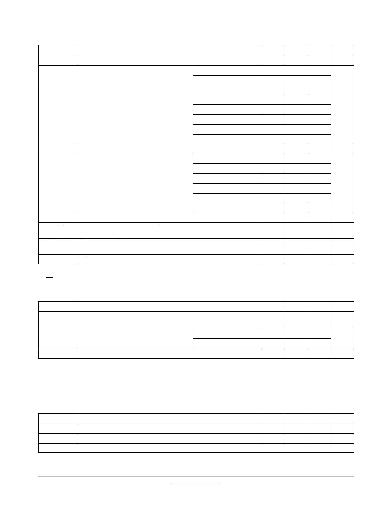
Table 5. M−BUS MODE − ELECTRICAL CHARACTERISTICS (Notes 4 and 5)
Symbol
Parameter
ΔVBR
ΔVCS
IBUS
ΔIBUS
ISTC
DISTC,SPACE
VB,PF
Voltage drop over bus rectifier (VBUS − VB) with RIDD = 4.02 kW
Voltage drop over CS1 (VB − VSTC)
RIDD ≤ 13 kW
RIDD ≤ 4.02 kW
Total current drawn from the bus, in Mark State RIDD = 30 kW
RIDD = 13 kW
RIDD = 8.45 kW
RIDD = 6.19 kW
RIDD = 4.87 kW
RIDD = 4.02 kW
Bus current stability (over ΔVBUS = 10 V, RX/RXI = mark)
Idle current available for the application to draw
from STC and VDD (including current drawn from
VDD)
RIDD = 30 kW
RIDD = 13 kW
RIDD = 8.45 kW
RIDD = 6.19 kW
RIDD = 4.87 kW
RIDD = 4.02 kW
Additional current available for the application when transmitting a space
Threshold voltage on VB to trigger PF
VPF,OH
PF voltage high (IPF = −100 mA)
VPF, OL
PF voltage low (Note 6) (IPF = 50 mA)
4. All voltages are referenced to GND
5. RIDD resistor with 1% accuracy
6. PF pin is pulled down with an on−chip resistor of typically 2 MW
Min
1.30
1.70
0.88
2.10
3.10
4.20
5.30
6.50
−
VSTC
+0.3
VIO −
0.6
0
Typ Max Unit
1.25 V
V
1.30
2.70
4.10
5.50
6.80
8.20
0.2
1.00
2.30
3.60
4.80
6.10
7.40
250
1.50
3.00
4.50
6.00
7.50
9.00
2
1.20
2.60
4.00
5.40
6.90
8.40
−
VSTC +
0.8
VIO
mA
%
mA
mA
V
V
0.6 V
Table 6. LOW POWER MODE − ELECTRICAL CHARACTERISTICS (Note 7)
Symbol
ΔVBR,LP
Parameter
Voltage drop over bus rectifier (VBUS − VB) with IBUS = 3 mA and external
Schottky diodes (Note 8)
Min Typ Max Unit
0.35 V
ISTC,LP
Max Current available for the application to draw RIDD (Note 9) = 30 kW
from STC and VDD (including current drawn
from VDD) (Note 10)
(Note 9) = 13 kW
2.0 2.3 2.7 mA
4.1 4.8 5.5
VSTC,CLAMP,LP Clamp voltage on pin STC (IDD < ISTC) (Note 11)
9.4 10.5 11.5
V
7. All voltages are referenced to GND
8. Forward voltage of 0.3 V max
9. Resistor with 1% accuracy
10. When configured in low power mode, the current limit of CS1 is set to 2 x the mark current level in M−BUS mode. The NCN5151 does not
behave as a current source but as current limiter because VSTC never reaches the STC clamp level.
11. The STC clamp function protects the STC capacitor in case 2WLPM or 3WLPM is accidentally enabled during regular M−Bus operation.
Table 7. GENERAL − ELECTRICAL CHARACTERISTICS (Note 12)
Symbol
Parameter
ICC Internal Supply Current (RIDD (Note 13)) = 13kW, RX/RXI = mark)
IIO Current drawn by the VIO pin
VRIDD
Voltage on RIDD pin
12. All voltages are referenced to GND
13. Resistor with 1% accuracy
Min Typ Max Unit
−
250 500
mA
−0.5 −
0.5 mA
1.15 1.2 1.25
V
www.onsemi.com
5
5 Page 
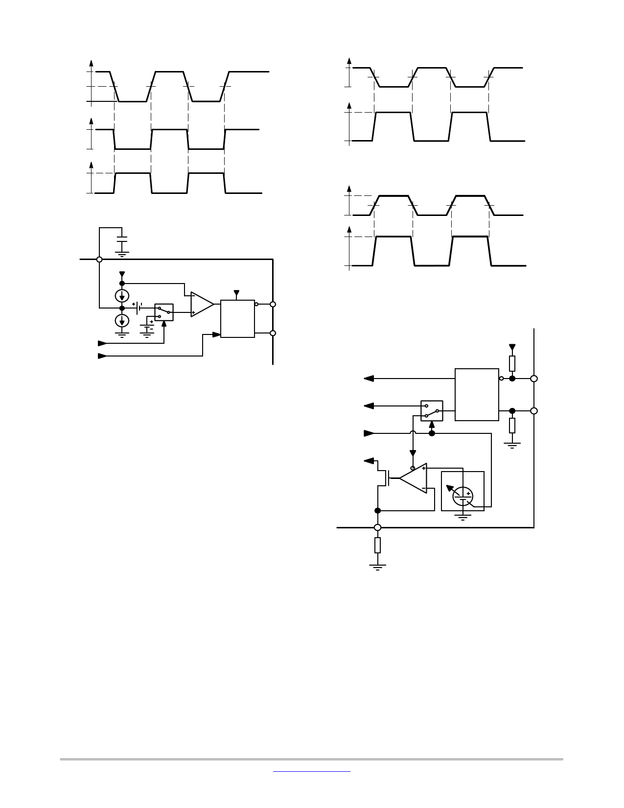
NCN5151
VBUS
VMARK
VT
VSPACE
VTX
VIO
VMARK = 21 … 42 V
VT = VMARK − 6 V
VSPACE = VMARK − 12 V
0
VTXI
VIO
0
PC20130419.1
Figure 6. Master to Slave Communication
CSC
SC
9 VB_INT
PC20130516.2
NCN5151
IDISCHARGE
LP_CTL
ECHO
ICHARGE
A
B
A: M−Bus Mode
B: 2&3Wire LPM
VIO_BUF
12 TX
Encoding
11 TXI
Figure 7. Receiver Block
Communication, Slave to Master
M−BUS communication from slave to master uses bus
current level modulation while the voltage remains constant.
This current modulation can be controlled from either the
RX or RXI pin as shown in Figures 8 and 9. When
transmitting a space (“0”), the current modulator will draw
an additional current from the bus. This current can be set
with a programming resistor RRIS. To achieve the space
current required the M−BUS standard, RRIS should be
100 W. A simplified schematic of the transmitter is shown in
Figure 10.
Because the M−BUS protocol is specified as half−duplex,
an echo function will cause the transmitted signal on RX or
RXI to appear on the receiver outputs TX and TXI. Should
the master attempt to send at the same time, the bitwise
added signal of both sources will appear on these pins,
resulting in invalid data.
VRX
VIO
0
IBUS
ISPACE
ISPACE = IMARK + 15 mA
IMARK
IMARK = N unit loads
PC20130514.5
Figure 8. Slave to Master Communication Driving RX
VRX
VIO
0
IBUS
ISPACE
ISPACE = IMARK + 15 mA
IMARK
IMARK = N unit loads
PC20130514.6
Figure 9. Slave to Master Communication Driving RXI
VIO_BUF
ECHO
LP_TX
LP_CTL
VB_IN
A: M−Bus/2WLP Mode
B: 3−Wire LP Mode
B
A
Decoding
17 RX
18 RXI
CS _TX
M−Bus: 1.5V
2−Wire LP: 1V
20
RIS
R IS
NCN5151
PC20130516.1
Figure 10. Transmitter Block
www.onsemi.com
11
11 Page | ||
| Páginas | Total 20 Páginas | |
| PDF Descargar | [ Datasheet NCN5151.PDF ] | |
Hoja de datos destacado
| Número de pieza | Descripción | Fabricantes |
| NCN5150 | Wired M-BUS Slave Transceiver | ON Semiconductor |
| NCN5151 | Wired M-BUS Slave Transceiver | ON Semiconductor |
| Número de pieza | Descripción | Fabricantes |
| SLA6805M | High Voltage 3 phase Motor Driver IC. |
Sanken |
| SDC1742 | 12- and 14-Bit Hybrid Synchro / Resolver-to-Digital Converters. |
Analog Devices |
|
DataSheet.es es una pagina web que funciona como un repositorio de manuales o hoja de datos de muchos de los productos más populares, |
| DataSheet.es | 2020 | Privacy Policy | Contacto | Buscar |
