|
|
PDF NCP6914 Data sheet ( Hoja de datos )
| Número de pieza | NCP6914 | |
| Descripción | 5 Channel PMIC: 1 DCDC Converter and 4 LDOs | |
| Fabricantes | ON Semiconductor | |
| Logotipo | ||
Hay una vista previa y un enlace de descarga de NCP6914 (archivo pdf) en la parte inferior de esta página. Total 30 Páginas | ||
|
No Preview Available !
NCP6914
5 Channel PMIC: 1 DCDC
Converter and 4 LDOs
The NCP6914 integrated circuits are part of the ON Semiconductor
mini power management IC family (PMIC). They are optimized to
supply battery powered portable application sub−systems such as
camera function and microprocessors. These devices integrate 1 high
efficiency 800 mA Step−down DC to DC converter with DVS
(Dynamic Voltage Scaling) and four low−dropout (LDO) voltage
regulators in a WLCSP20 1.77 x 2.06 mm package.
Features
• 1 DCDC Converter (3 MHz, 1 mH/10 mF, 800 mA)
♦ Peak Efficiency 95%
♦ Programmable Output Voltage from 0.6 V to 3.3 V by 12.5 mV
Steps
• 4 Low Noise − Low Dropout Regulators (300 mA)
♦ Programmable Output Voltage from 1.0 V to 3.3 V by 50 mV
Steps
♦ 50 mVrms Typical Low Output Noise
• Control
♦ 400 kHz / 3.4 MHz I2C Compatible
♦ Hardware Enable Pin
♦ Power Good and Interrupt Output Pin
♦ External Synchronization
♦ Customizable Power Up Sequencer
• Extended Input Voltage Range 2.3 V to 5.5 V
• Optimized Power Efficiency
♦ 72 mA Very Low Quiescent Current at No Load
♦ Less than 1 mA Off Mode Current
• Small Footprint: Package 1.77 x 2.06 mm WLCSP
• These are Pb−Free Devices
Typical Applications
• Cellular Phones
• Digital Cameras
• Personal Digital Assistant and Portable Media Player
• GPS Systems
Battery or
System Supply
AVIN
B3
1 .0 uF
100 nF
AGND
VBG
B4
A4
Processor or
System Supply
Processor
Interrupt
Processor
I@C
Power State
Indicator
HWEN C1
INTB D3
SDA C2
SCL D2
SYNC C3
PG B2
NCP6914
Core
Power Up
Sequencer
Thermal
Protection
Enabling
Interrupt
I2C
Clocking
Supply
Monitoring
DCDC 1
800 mA
LDO 1
300 mA
LDO 2
300 mA
LDO 3
300 mA
LDO 4
300 mA
D1 PVIN1
E2 SW1
E3 FB1
E1 PGND1
4.7 uF
System Supply
1 uH
DCDC1 Out
10 uF
C4 VOUT1
D4 VIN12
E4 VOUT2
A2 VIN3
A3 VOUT3
A1 VIN4
B1 VOUT4
Rev 1. 00
System or
DCDC
Supply
System or
DCDC
Supply
System or
DCDC
Supply
LDO1 Out
2 .2uF
LDO2 Out
2 .2uF
LDO3 Out
2 .2uF
LDO4 Out
2 .2 uF
Figure 1. Application Schematic
http://onsemi.com
MARKING
DIAGRAM*
WLCSP20
CASE 567CV
6914Ax
AWLYWW
G
x = A for NCP6914AA
= B for NCP6914AB
= D for NCP6914AD
A = Assembly Location
WL = Wafer Lot
Y = Year
WW = Work Week
G = Pb−Free Package
(Pb−Free indicator, “G” or microdot “ G”, may or may
not be present.)
123 4
A
VIN4
VIN3
VOUT3
VBG
B VOUT4
PG
AVIN
AGND
C
HWEN
SDA
SYNC
VOUT1
D PVIN1 SCL
INTB
VIN12
E PGND1 SW1
FB1 VOUT2
(Top View)
20−Pin 1.77 x 2.06 mm WLCSP, 0.40 mm Pitch
ORDERING INFORMATION
See detailed ordering and shipping information in the package
dimensions section on page 35 of this data sheet.
© Semiconductor Components Industries, LLC, 2014
April, 2014 − Rev. 10
1
Publication Order Number:
NCP6914/D
1 page 
NCP6914
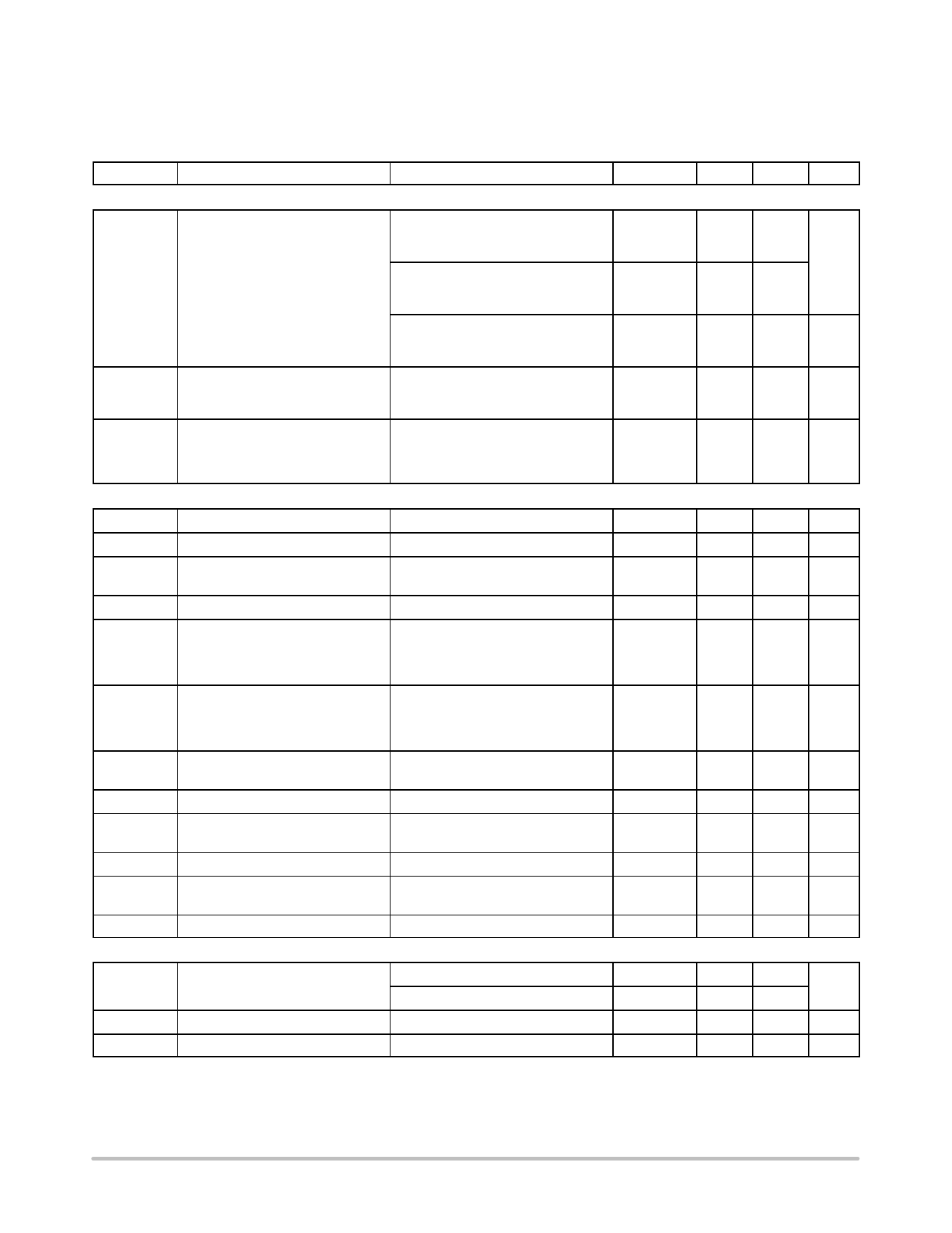
Table 4. ELECTRICAL CHARACTERISTICS
Min & Max Limits apply for TJ up to +125°C unless otherwise specified. AVIN = PVIN1 = VIN12 = VIN3 = VIN4 = 3.6 V (unless otherwise
noted). DCDC Output Voltage = 1.2 V, LDO1&2 = 1.8 V, LDO3&4 = 2.8 V, Typical values are referenced to TJ = + 25°C and default
configuration (Note 10)
Symbol
Parameter
Conditions
Min Typ Max Unit
SUPPLY CURRENT: PINS AVIN − PVIN1
IQ Operating Quiescent Current
ISLEEP
Product Sleep Mode Current
IOFF
Product Off Current
DCDC Converter
DCDC on − no load − no switching
LDOs off
TA = up to +85°C
DCDC on − no load − no switching
LDOs on − no load
TA = up to +85°C
DCDC Off
All LDOs on − no load
TA = up to +85°C
HWEN on
DCDC and all LDOs off
TA = up to +85°C
HWEN off
I2C interface disabled
VIN = 2.3 V to 5.5 V
TA = up to +85°C
−
−
−
−
−
32 70 mA
72 190
55 100 mA
7 15 mA
0.1 2.0 mA
PVIN
IOUTMAX
DVOUT
FSW
RONHS
Input Voltage Range
Maximum Output Current
Output Voltage DC Error
Switching Frequency
P−Channel MOSFET On Res-
istance
Io = 300 mA, PWM mode
TA = up to +85°C
From PVIN1 to SW1, TA = up to +85°C
Guarantee by design and
characterization, production tested at
Vin = 3.6 V
2.3
0.8
−1
2.7
−
− 5.5 V
− −A
0 1%
− 3.3 MHz
230 − mW
RONLS
N−Channel MOSFET On Res-
istance
From SW1 to PGND1, TA up to 85°C
Guarantee by design and
characterization, production tested at
Vin=3.6 V
−
200 − mW
IPK
D
tSTART
Peak Inductor Current
Load Regulation
Line Regulation
Maximum Duty Cycle
Soft−Start Time
Open loop
2.3 V ≤ PVIN ≤ 5.5 V
IOUT from 300 mA to IOUTMAX
IOUT = 300 mA
2.3 V ≤ VIN ≤ 5.5 V
Time from I2C command ACK to
90% of Output Voltage
1.0 1.3 1.6 A
− 5 − mV/A
− 0 − %/V
−
100 −
%
− − 1 ms
RDISDCDC DCDC Active Output Discharge
LDO1 AND LDO2
− 7 −W
VIN12
LDO1 and LDO2 input voltage
Range 300 mA load
VOUT ≤ 1.3 V, IOUT = 300 mA
VOUT > 1.3 V, IOUT = 300 mA
1.7
Vout + VDROP
−
−
5.5
V
5.5
IOUTMAX1,2 Maximum Output Current
300 − − mA
ISC1,2
Short Circuit Protection
360 − 700 mA
9. Devices that use non−standard supply voltages which do not conform to the intent I2C bus system levels must relate their input levels
to the VDD voltage to which the pull−up resistors RP are connected.
10. Refer to the Application Information section of this data sheet for more details.
11. Guaranteed by design and characterized.
http://onsemi.com
5
5 Page 
NCP6914
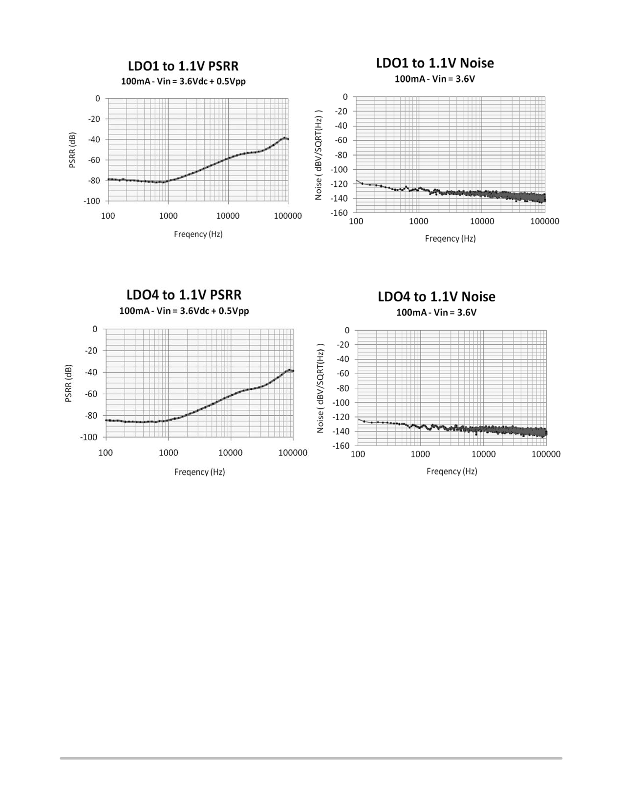
Figure 16. LDO1 PSRR
Figure 17. LDO1 Outputs Noise
Figure 18. LDO4 PSRR
Figure 19. LDO4 Output Noise
http://onsemi.com
11
11 Page | ||
| Páginas | Total 30 Páginas | |
| PDF Descargar | [ Datasheet NCP6914.PDF ] | |
Hoja de datos destacado
| Número de pieza | Descripción | Fabricantes |
| NCP691 | Very Low Dropout Regulator (VLDO) | ON Semiconductor |
| NCP6914 | 5 Channel PMIC: 1 DCDC Converter and 4 LDOs | ON Semiconductor |
| Número de pieza | Descripción | Fabricantes |
| SLA6805M | High Voltage 3 phase Motor Driver IC. |
Sanken |
| SDC1742 | 12- and 14-Bit Hybrid Synchro / Resolver-to-Digital Converters. |
Analog Devices |
|
DataSheet.es es una pagina web que funciona como un repositorio de manuales o hoja de datos de muchos de los productos más populares, |
| DataSheet.es | 2020 | Privacy Policy | Contacto | Buscar |
