|
|
PDF HD74HC620 Data sheet ( Hoja de datos )
| Número de pieza | HD74HC620 | |
| Descripción | Octal Bus Transceivers | |
| Fabricantes | Renesas | |
| Logotipo |  |
|
Hay una vista previa y un enlace de descarga de HD74HC620 (archivo pdf) en la parte inferior de esta página. Total 12 Páginas | ||
|
No Preview Available !
HD74HC620, HD74HC623
Octal Bus Transceivers (with inverted 3-state outputs)
Octal Bus Transceivers (with 3-state outputs)
REJ03D0636-0200
(Previous ADE-205-516)
Rev.2.00
Mar 30, 2006
Description
This octal bus transceiver is designed for asynchronous two-way communication between data buses. The control
function implementation allows for maximum flexibility in timing.
This device allows data transmission from the A bus to the B bus or from the B bus to the A bus depending upon the
logic levels at the enable inputs (GBA and GAB).
The enable inputs can be used to disable the device so that the buses are effectively isolated.
The dual-enable configuration gives these devices the capability to store data by simultaneous enabling of GBA and
GAB. Each output reinforces its input in this transceiver configuration. Thus, when both control inputs are enabled and
all other data sources to the two sets of bus lines are at high impedance, both sets of bus lines (16 in all) will remain at
their last states. The 8-bit codes appearing on the two sets of buses will be identical for the HD74HC623 or
complementary for the HD74HC620.
Features
• High Speed Operation: tpd (Bus to Bus) = 12 ns typ (CL = 50 pF)
• High Output Current: Fanout of 15 LSTTL Loads (QA to QH outputs)
• Wide Operating Voltage: VCC = 2 to 6 V
• Low Input Current: 1 µA max
• Low Quiescent Supply Current: ICC (static) = 4 µA max (Ta = 25°C)
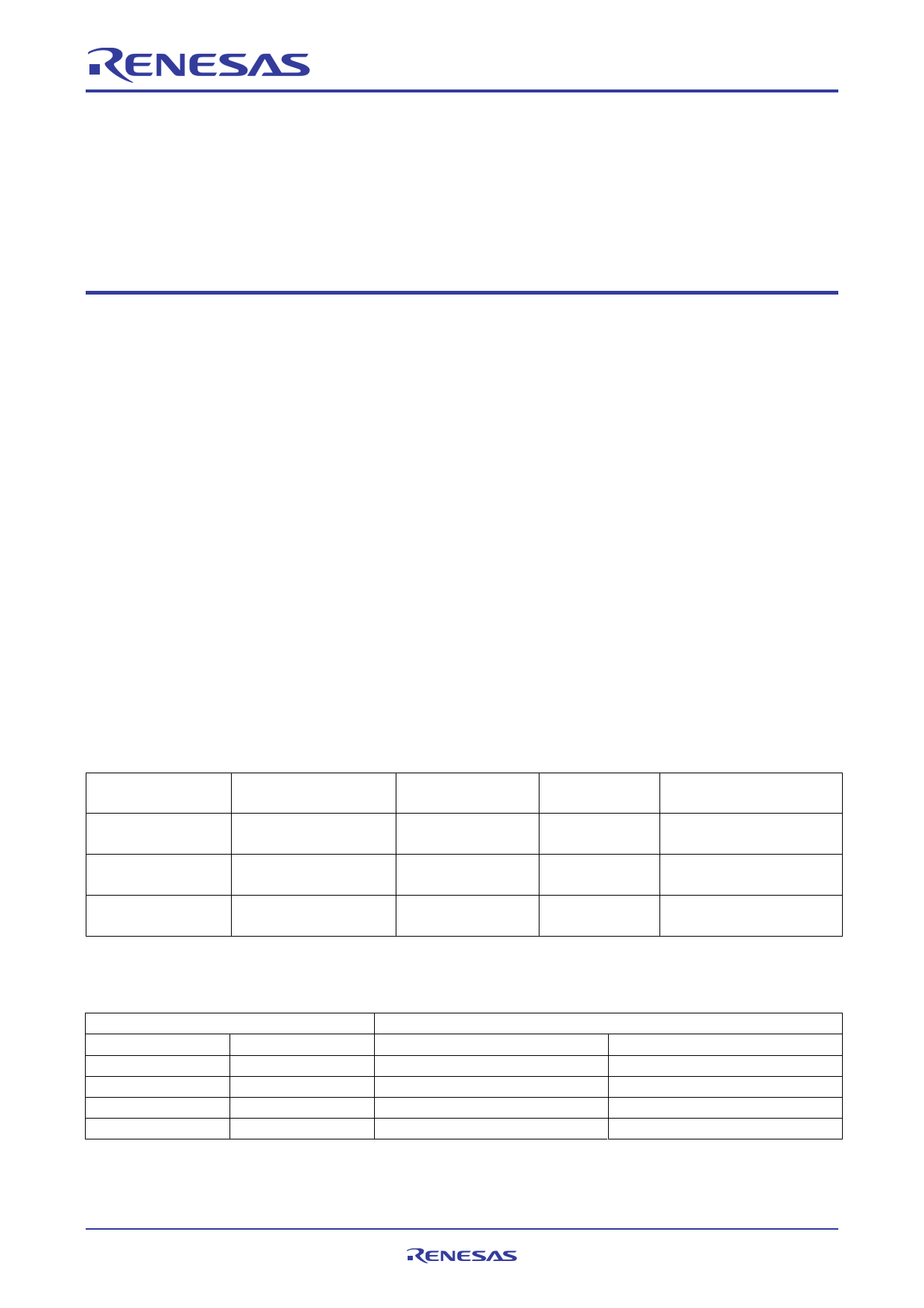
• Ordering Information
Part Name
Package Type
Package Code
(Previous Code)
Package
Abbreviation
HD74HC620P
DILP-20 pin
PRDP0020AC-B
(DP-20NEV)
P
HD74HC620FPEL
HD74HC623FPEL
SOP-20 pin (JEITA)
PRSP0020DD-B
(FP-20DAV)
FP
HD74HC620RPEL
HD74HC623RPEL
SOP-20 pin (JEDEC)
PRSP0020DC-A
(FP-20DBV)
RP
Note: Please consult the sales office for the above package availability.
Taping Abbreviation
(Quantity)
—
EL (2,000 pcs/reel)
EL (1,000 pcs/reel)
Function Table
Enable Inputs
GBA
GAB
LL
HH
HL
LH
Operation
HD74HC620
HD74HC623
B data to A bus
B data to A bus
A data to B bus
A data to B bus
Isolation
Isolation
B data to A bus, A data to B bus B data to A bus, A data to B bus
Rev.2.00 Mar 30, 2006 page 1 of 11
1 page 
HD74HC620, HD74HC623
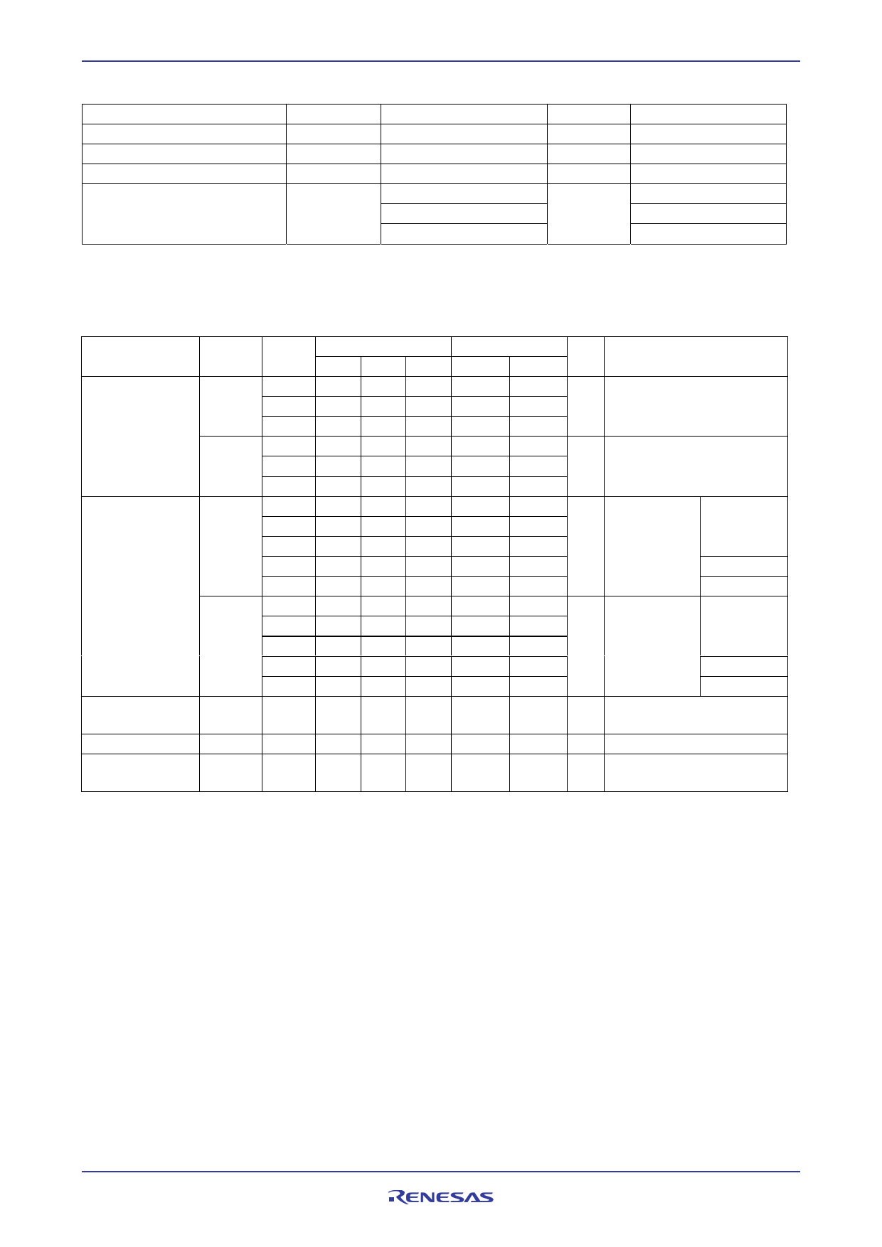
Recommended Operating Conditions
Item
Symbol
Ratings
Supply voltage
Input / Output voltage
VCC
VIN, VOUT
2 to 6
0 to VCC
Operating temperature
Ta –40 to 85
Input rise / fall time*1
0 to 1000
tr, tf 0 to 500
0 to 400
Note: 1. This item guarantees maximum limit when one input switches.
Waveform: Refer to test circuit of switching characteristics.
Unit
V
V
°C
ns
Conditions
VCC = 2.0 V
VCC = 4.5 V
VCC = 6.0 V
Electrical Characteristics
Item
Input voltage
Output voltage
Off-state output
current
Input current
Quiescent supply
current
Symbol
VIH
VIL
VOH
VOL
IOZ
Iin
ICC
VCC (V)
2.0
4.5
6.0
2.0
4.5
6.0
2.0
4.5
6.0
4.5
6.0
2.0
4.5
6.0
4.5
6.0
6.0
6.0
6.0
Ta = 25°C
Min Typ Max
1.5 — —
3.15 — —
4.2 — —
— — 0.5
— — 1.35
— — 1.8
1.9 2.0 —
4.4 4.5 —
5.9 6.0 —
4.18 — —
5.68 — —
— 0.0 0.1
— 0.0 0.1
— 0.0 0.1
— — 0.26
— — 0.26
— — ±0.5
— — ±0.1
— — 4.0
Ta = –40 to+85°C
Min Max Unit
Test Conditions
1.5 — V
3.15 —
4.2 —
— 0.5 V
— 1.35
— 1.8
1.9 — V Vin = VIH or VIL IOH = –20 µA
4.4 —
5.9 —
4.13 —
IOH = –6 mA
5.63 —
IOH = –7.8 mA
— 0.1 V Vin = VIH or VIL IOL = 20 µA
— 0.1
— 0.1
— 0.33
IOL = 6 mA
— 0.33
IOL = 7.8 mA
— ±5.0 µA Vin = VIH or VIL,
Vout = VCC or GND
— ±1.0 µA Vin = VCC or GND
— 40 µA Vin = VCC or GND, Iout = 0 µA
Rev.2.00 Mar 30, 2006 page 5 of 11
5 Page 
HD74HC620, HD74HC623
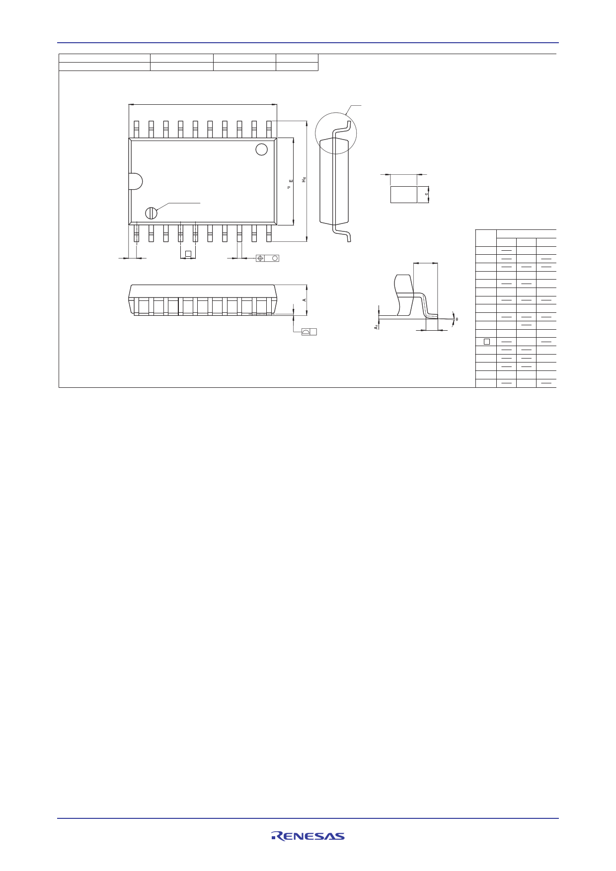
JEITA Package Code
P-SOP20-7.5x12.8-1.27
RENESAS Code
PRSP0020DC-A
Previous Code
FP-20DBV
MASS[Typ.]
0.52g
*1 D
20
11
Index mark
1
Z
e
*3 b p
10
xM
y
F
bp
NOTE)
1. DIMENSIONS"*1 (Nom)"AND"*2"
@ DO NOT INCLUDE MOLD FLASH.
2. DIMENSION"*3"DOES NOT
@ INCLUDE TRIM OFFSET.
Terminal cross section
( Ni/Pd/Au plating )
L1
Detail F
L
Reference Dimension in Millimeters
Symbol Min Nom Max
D 12.80 13.2
E 7.50
A2
A1 0.10 0.20 0.30
A 2.65
bp 0.34 0.40 0.46
b1
c 0.20 0.25 0.30
θ c1
θ 0°
8°
HE 10.00 10.40 10.65
e 1.27
x 0.12
y 0.15
Z 0.935
L 0.40 0.70 1.27
L1 1.45
Rev.2.00 Mar 30, 2006 page 11 of 11
11 Page | ||
| Páginas | Total 12 Páginas | |
| PDF Descargar | [ Datasheet HD74HC620.PDF ] | |
Hoja de datos destacado
| Número de pieza | Descripción | Fabricantes |
| HD74HC620 | Octal Bus Transceivers(with inverted 3-state outputs) | Hitachi Semiconductor |
| HD74HC620 | Octal Bus Transceivers | Renesas |
| HD74HC623 | Octal Bus Transceivers(with inverted 3-state outputs) | Hitachi Semiconductor |
| HD74HC623 | Octal Bus Transceivers | Renesas |
| Número de pieza | Descripción | Fabricantes |
| SLA6805M | High Voltage 3 phase Motor Driver IC. |
Sanken |
| SDC1742 | 12- and 14-Bit Hybrid Synchro / Resolver-to-Digital Converters. |
Analog Devices |
|
DataSheet.es es una pagina web que funciona como un repositorio de manuales o hoja de datos de muchos de los productos más populares, |
| DataSheet.es | 2020 | Privacy Policy | Contacto | Buscar |
