|
|
|
PDF CLC412AIB Data sheet ( Hoja de datos )
| Número de pieza | CLC412AIB | |
| Descripción | Dual Wideband Video Op Amp | |
| Fabricantes | National Semiconductor | |
| Logotipo | ||
Hay una vista previa y un enlace de descarga de CLC412AIB (archivo pdf) en la parte inferior de esta página. Total 12 Páginas | ||
|
No Preview Available !
N
CLC412
Dual Wideband Video Op Amp
June 1999
General Description
The CLC412 combines a high-speed complementary bipolar process
with National's current-feedback topology to produce a very high-
speed dual op amp. The CLC412 provides a 250MHz small-signal
bandwidth at a gain of +2V/V and a 1300V/µs slew rate while
consuming only 50mW per amplifier from ±5V supplies.
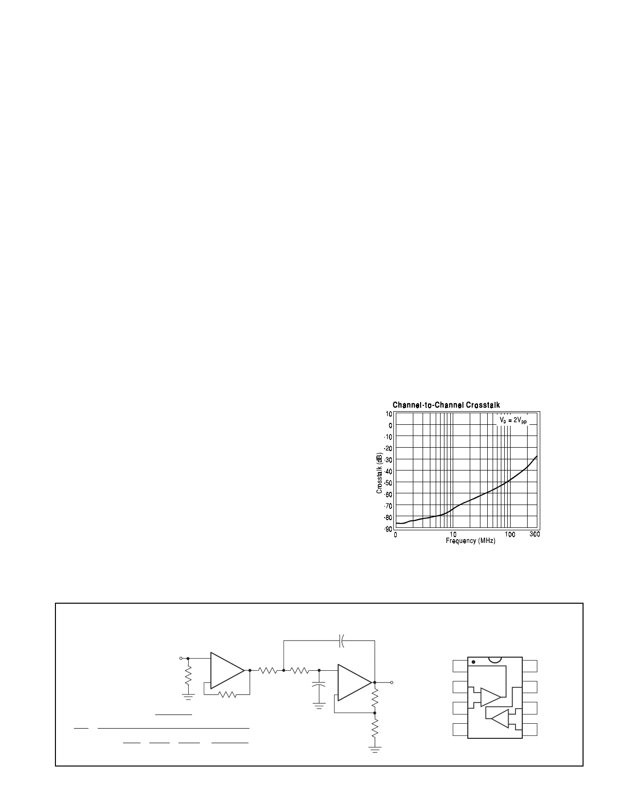
The CLC412 offers exceptional video performance with its 0.02%
and 0.02° differential gain and phase errors for NTSC and PAL video
signals while driving one back terminated 75Ω load. The CLC412
also offers a flat gain response of 0.1dB to 30MHz and very low
channel-to-channel crosstalk of -76dB at 10MHz. Additionally, each
amplifier can deliver a 70mA continuous output current. This level of
performance makes the CLC412 an ideal dual op amp for high-
density broadcast-quality video systems.
The CLC412's two very well-matched amplifiers support a number of
applications such as differential line drivers and receivers. In
addition, the CLC412 is well suited for Sallen Key active filters in
applications such as anti-aliasing filters for high-speed A/D
converters. Its small 8-pin SOIC package, low power requirement,
low noise and distortion allow the CLC412 to serve portable RF
applications such as IQ-channels.
The CLC412 is available in the following versions.
CLC412AJP
CLC412AJE
CLC412AIB
CLC412A8B
-40°C to +85°C
-40°C to +85°C
-40°C to +85°C
-55°C to +125°C
CLC412A8L-2A
-55°C to +125°C
CLC412AMC
-55°C to +125°C
DESC SMD number: 5962-94719
8-pin Plastic DIP
8-pin Plastic SOIC
8-pin CERDIP
8-pin CERDIP,
MIL-STD-883, Level B
20-pin LCC,
MIL-STD-883, Level B
dice,
MIL-STD-883, Level B
Features
s Wide bandwidth: 330MHz (Av=+1V/V)
250MHz (Av=+2V/V)
s 0.1dB gain flatness to 30MHz
s Low power: 5mA/channel
s Very low diff. gain, phase: 0.02%, 0.02°
s -76dB channel-to-channel crosstalk
(10MHz)
s Fast slew rate: 1300V/µs
s Unity-gain stable
Applications
s HDTV, NTSC & PAL video systems
s Video switching and distribution
s IQ amplifiers
s Wideband active filters
s Cable drivers
s DC coupled single-to-differential conversions
Typical Application
Sallen-Key Low-Pass Filter
Vin
+
R ½CLC412
in
-
R1
Ko Rf
Vout =
R1R2C1C2
Vin
s2
+
s
1
+
1
+
1−
K9
+
1
R1C1 R2C2 R2C2 R1R2C1C2
© 1999 National Semiconductor Corporation
Printed in the U.S.A.
Pinout
C1 DIP & SOIC
R2
+
Vout
Vout1 1
8 +Vcc
C2 ½CLC412
- Rf
Vinv1 2
-
+
7 Vout2
Vnon-inv1 3
- 6 Vinv2
Rg -Vcc 4
+
5 Vnon-inv2
http://www.national.com
1 page 
+Vcc + C3
Vin
Rin
Rg
C1
+
½CLC412
-
C2
+
-Vcc
C4
Rf
Vout
Ro
Rf
+Vcc
+ C3
Vin
Rg
C1
-
½CLC412
+
C2
Rb
+
-Vcc
C4
Vout
Ro
Figure 1
Application Introduction
Offered in an 8-pin package for reduced space and cost,
the wideband CLC412 dual current-feedback op amp
provides closely matched DC & AC electrical performance
characteristics making the part an ideal choice for
wideband signal processing. Applications such as
broadcast-quality video systems, IQ amplifiers, filter
blocks, high-speed peak detectors, integrators and
transimpedance amplifiers will all find superior
performance in the CLC412 dual op amp.
Feedback Resistor Selection
The loop gain and frequency response for a current-
feedback operational amplifier is determined largely by
the feedback resistor, Rf. The Electrical Characteristics
and Typical Performance plots specify an Rf of 634Ω, a
gain of +2V/V and operation with ±5V power supplies
(unless otherwise stated). Generally, lowering Rf from its
recommended value will peak the frequency response
and extend the bandwidth while increasing its value will
roll off the response. Reducing the value of Rf too far
below its recommended value will cause overshoot,
ringing and eventually oscillation.
Figure 2
and phase response to the value of the feedback resistor,
Rf. For more information see Application Note OA-13
which describes the relationship between Rf and closed-
loop frequency response.
When configuring the CLC412 for other inverting or non-
inverting gains, it is necessary to adjust the value of the
feedback resistor in order to optimize the device’s
frequency and phase response. The two plots below
provide the means of selecting the recommended
feedback-resistor value for both inverting and non-
The plot above labeled "Frequency Response vs. Rf"
shows the CLC412’s frequency and phase response as
Rf is varied while the gain remains constant at +2V/V
(RL=100Ω). This plot shows that one particular value of
Rf will optimize the frequency and phase response at the
specified gain setting, i.e. 634Ω at a gain of +2V/V.
Current-feedback op amps, unlike voltage-feedback op
amps, have a direct relationship between their frequency
inverting gain selections. Both plots show the value of Rf
approaching a non-zero minimum (dashed line) at high
gains, which is characteristic of current-feedback op
amps, while the linear portion of the two (solid) curves
(i.e. -5>Av>+6) results from the limitation placed on Rg
(i.e. Rg ≥50Ω). This limitation is due to the desire to keep
Rg greater in value than that of the inverting input
resistance. Therefore, the resulting small-signal
5 http://www.national.com
5 Page 
This page intentionally left blank.
11 http://www.national.com
11 Page | ||
| Páginas | Total 12 Páginas | |
| PDF Descargar | [ Datasheet CLC412AIB.PDF ] | |
Hoja de datos destacado
| Número de pieza | Descripción | Fabricantes |
| CLC412AIB | Dual Wideband Video Op Amp | National Semiconductor |
| Número de pieza | Descripción | Fabricantes |
| SLA6805M | High Voltage 3 phase Motor Driver IC. |
Sanken |
| SDC1742 | 12- and 14-Bit Hybrid Synchro / Resolver-to-Digital Converters. |
Analog Devices |
|
DataSheet.es es una pagina web que funciona como un repositorio de manuales o hoja de datos de muchos de los productos más populares, |
| DataSheet.es | 2020 | Privacy Policy | Contacto | Buscar |