|
|
|
PDF BD81842MUV-M Data sheet ( Hoja de datos )
| Número de pieza | BD81842MUV-M | |
| Descripción | Automotive Panel Power Management IC | |
| Fabricantes | ROHM Semiconductor | |
| Logotipo | ||
Hay una vista previa y un enlace de descarga de BD81842MUV-M (archivo pdf) en la parte inferior de esta página. Total 30 Páginas | ||
|
No Preview Available !
Datasheet
Power Supply IC Series for TFT-LCD Panels
Automotive Panel Power Management IC
BD81842MUV-M
●General Description
The BD81842MUV-M is a power management IC for
TFT-LCD panels which are used in car navigation,
in-vehicle center panel, and instrument cluster.
Incorporates high-power FET with low on resistance for
large currents that employ high-power packages, thus
driving large current loads while suppressing the
generation of heat. A charge pump controller is
incorporated as well, thus greatly reducing the number
of application components. Also Gate Shading Function
is included.
●Key Specifications
Input voltage range :
AVDD Output voltage range :
SRC Output voltage range :
VCOM Output current :
Oscillator Frequency :
Operating temperature range :
2.0V to 5.5V
6.0V to 18V
12V to 34V
200mA (Typ.)
2.1MHz (Typ.)
-40℃ to +105℃
●Special Characteristics
FB Regulation voltage :
±3% (Ta=-40~105℃)
Oscillator Frequency : ±10.5% (Ta=-40~105℃)
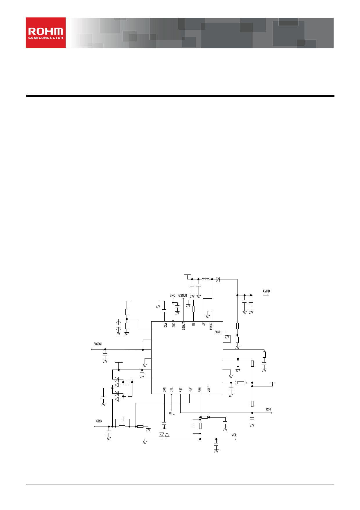
●Typical Application Circuit (TOP VIEW)
●Applications
TFT-LCD Panels which are used in car navigation,
in-vehicle center panel, and instrument cluster.
●Features
AEC-Q100 Qualified(Note 1)
Boost DC/DC converter; 18 V / 2.5 A switch current.
Switching frequency: 2.1 MHz
Operational Amplifier (short current 200mA)
Incorporates Positive / Negative Charge-pump
Controllers.
Gate Shading Function
Protection circuits:
Under Voltage Lockout
Protection Circuit
Thermal Shutdown Circuit (Latch Mode)
Over Current Protection Circuit (AVDD)
Timer Latch Mode Short Circuit Protection (AVDD
SRC /VGL)
Over / Under Voltage Protection Circuit for Boost
DC/DC Output
No SCP time included (185ms from UVLO-off)
(Note1: Grade 2)
●Package
VQFN24SV4040
TDK
VIN SLF7055T-100M2R5(10μH,2.5A)
W(Typ.) x D(Typ.) x H(Max.)
4.0mm x 4.0mm x 1.0mm
10uF
10uF
RSX301LA-30
10V/0.5Amax
AVDD
5.5V
VCOM
AVDD
18k
22k
1uF
AVDD
0.1uF
DA227
0.1uF
0.1uF
DA227
33nF
24
SRC GSOUT
1k
23 22
21 20
1
INP
2
INN
3
VCOM
4
AGND1
5
AVDD
6
DRP
19
18
PGND
FB 17
16
COMP
15
RSTIN
14
AGND2
VIN 13
78
9 10
CTL
11 12
10uF 10uF 10uF
91k
13k
24k
10k 10k 2.2nF
VIN
3.3V
1uF
10k RST
20V/20mA max
SRC
1uF 150k
10k
0.1uF
1uF
16k 0.22μF
120k
VGL
DA227
-7.1V/20mA max
1uF
Figure 1. Application Circuit
○Product structure:Silicon monolithic integrated circuit ○This product is not designed for protection against radioactive rays
www.rohm.com
© 2015 ROHM Co., Ltd. All rights reserved.
TSZ22111・14・001
1/31
TSZ02201-0313AAF00540-1-2
23. Jun. 2016 Rev.002
1 page 
BD81842MUV-M
Datasheet
●Main Block Function
・Boost Converter
A controller circuit for DC/DC boosting.
The switching duty is controlled so that the feedback voltage FB is set to 1.25 V (typ.).
A soft start operates at the time of starting.
・Positive Charge Pump
A controller circuit for the positive-side charge pump.
The switching amplitude is controlled so that the feedback voltage FBP will be set to 1.25 V (typ.).
・Negative Charge Pump
A controller circuit for the negative-side charge pump.
The switching amplitude is controlled so that the feedback voltage FBN will be set to 0.265 V (Typ.).
・Gate Shading Controller
A controller circuit for P-MOS FET Switch
The GSOUT switching synchronize with CTL input.
Please input voltage below VIN to CTL.
When VIN drops below UVLO threshold or RST=Low(=RSTIN<1.25V), GSOUT is pulled High(=SRC).
・VCOM
1-channel operational amplifier block.
・Reset
An open-drain output(RST) refer from RSTIN voltage(up to threshold voltage 1.25V).
RST keeps High(need a pull-up resistor connected to VIN) dulling to 185ms from start-up.
・VREF
A block that generates internal reference voltage of 1.25V (Typ.).
VREF is keep High when the thermal/short-current-protection shutdown circuit.
・TSD/UVLO/OVP/UVP
The thermal shutdown circuit is shut down at an IC internal temperature of 160℃.
The under-voltage lockout protection circuit shuts down the IC when the VIN is 1.85 V (Typ.) or below.
The over-voltage protection circuit when the AVDD is 20 V (Typ.) or over.
The under-voltage protection circuit when the AVDD is 1.3 V (Typ.) or under
・Start-up Controller
A control circuit for the starting sequence.
Controls to start in order of VIN VGL AVDDSRC
(Please refer to Fig.27 of 16 page for details.)
www.rohm.com
© 2015 ROHM Co., Ltd. All rights reserved.
TSZ22111・15・001
5/31
TSZ02201-0313AAF00540-1-2
23. Jun. 2016 Rev.002
5 Page 
BD81842MUV-M
●Electrical characteristic curves (Reference data)
(Unless otherwise specified VIN = 3.3V, AVDD = 10V and Ta=25℃)
Datasheet
Figure 12. COMP Sink Current
Figure 13. COMP Source Current
IAVDD
AVDD
Figure 14. Load Transient
Response Falling
IAVDD
AVDD
Figure 15. Load Transient
Response Rising
www.rohm.com
© 2015 ROHM Co., Ltd. All rights reserved.
TSZ22111・15・001
11/31
TSZ02201-0313AAF00540-1-2
23. Jun. 2016 Rev.002
11 Page | ||
| Páginas | Total 30 Páginas | |
| PDF Descargar | [ Datasheet BD81842MUV-M.PDF ] | |
Hoja de datos destacado
| Número de pieza | Descripción | Fabricantes |
| BD81842MUV-M | Automotive Panel Power Management IC | ROHM Semiconductor |
| Número de pieza | Descripción | Fabricantes |
| SLA6805M | High Voltage 3 phase Motor Driver IC. |
Sanken |
| SDC1742 | 12- and 14-Bit Hybrid Synchro / Resolver-to-Digital Converters. |
Analog Devices |
|
DataSheet.es es una pagina web que funciona como un repositorio de manuales o hoja de datos de muchos de los productos más populares, |
| DataSheet.es | 2020 | Privacy Policy | Contacto | Buscar |