|
|
|
PDF SJ7500P Data sheet ( Hoja de datos )
| Número de pieza | SJ7500P | |
| Descripción | Pulse Width Modulation | |
| Fabricantes | AUK | |
| Logotipo | ||
Hay una vista previa y un enlace de descarga de SJ7500P (archivo pdf) en la parte inferior de esta página. Total 11 Páginas | ||
|
No Preview Available !
Semiconductor
SJ7500/P
Pulse Width Modulation
◈ Description
The SJ7500 is a monolithic integrated circuit which includes all the necessary building
blocks for the design of pulse width modulate(PWM) switching power supplies, including
push-pull, bridge and series configuration. The precision of voltage reference is improved
up to ±1% through trimming and this provides a better output voltage regulation. The
device can operate at switching frequencies between 1KHz and 300KHz and output voltage
up to 23V. The SJ7500 is specified over an operating temperature range of -25℃~+85℃.
◈ Features
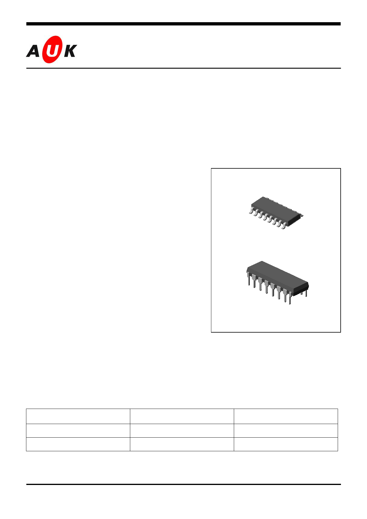
◈ Package Type
• Internal Regulator Provides a Stable 5V
Reference Supply Trimmed to ±1% Accuracy
• Uncommitted output transistors capable
of 200mA source or sink
• Internal protection from double pulsing of
out-puts with narrow pulse widths or with
supply voltages below specified limits
• Easily synchronized to other circuits
• Dead time control comparator
• Output control selects single-ended or
push-pull operation
• Operating temperature range : -25℃ ~ +85℃
• Halogen-Free Package is Available
• High Level ESD Protection : 400V(MM), 4KV(HBM)
◈ Application
SOP-16
DIP-16
• Charger
• SMPS
• Back Light Inverter
◈ Ordering Information
PKG Type
SJ7500
SJ7500P
Device Name
SOP-16
DIP-16
Marking
SJ7500
SJ7500P
KSD-I7D001-000
1
1 page 
SJ7500/P
INFORMATION
The basic oscillator(switching)frequency is controlled by an external resistor (Rt) and
capacitor(Ct). The relationship between the values of Rt Ct and frequency is shown in.
The level of the sawtooth wave form is compared with an error voltage by the pulse width
modulated comparator. The output of the PWM Comparator directs the pulse steering flip
flop and the output control logic.
The error voltage is generated by the error amplifier. The error amplifier boosts the voltage
difference between the output and the 5V internal reference. See Figure7 for error amp
sensing techniques. The second error amp is typically used to implement current limiting.
The output control logic (Pin13) selects either push-pull or single-ended operation of the
output transistors (see Figure6). The dead time control prevents on-state overlap of the
output transistors as can be seen is Figure5. The dead time is approximately 3 to 5% of the
total period if the dead time control(pin4) is grounded. This dead time can be increased by
connecting the dead time control to a voltage up to 5 V. The frequency response of the
error amps can be modified by using external resistors and capacitors. These components
are typically connected between the compensation terminal (pin3) and the inverting input
of the error amps(pin2 or pin15). The switching frequency of two or more SJ7500 circuits
can be synchronized. The timing capacitor, Ct is connected as shown in Figure8. Charging
current is provided by the master circuit. Discharging is through all the circuits slaved to
the master. Rt is required only for the master circuit.
Operating Waveform
KSD-I7D001-000
5
5 Page 
SJ7500/P
The AUK Corp. products are intended for the use as components in general electronic
equipment (Office and communication equipment, measuring equipment, home
appliance, etc.).
Please make sure that you consult with us before you use these AUK Corp. products
in equipments which require high quality and / or reliability, and in equipments which
could have major impact to the welfare of human life(atomic energy control, airplane,
spaceship, transportation, combustion control, all types of safety device, etc.). AUK
Corp. cannot accept liability to any damage which may occur in case these AUK Corp.
products were used in the mentioned equipments without prior consultation with AUK
Corp..
Specifications mentioned in this publication are subject to change without notice.
KSD-I7D001-000
11
11 Page | ||
| Páginas | Total 11 Páginas | |
| PDF Descargar | [ Datasheet SJ7500P.PDF ] | |
Hoja de datos destacado
| Número de pieza | Descripción | Fabricantes |
| SJ7500 | Pulse Width Modulation | AUK |
| SJ7500P | Pulse Width Modulation | AUK |
| Número de pieza | Descripción | Fabricantes |
| SLA6805M | High Voltage 3 phase Motor Driver IC. |
Sanken |
| SDC1742 | 12- and 14-Bit Hybrid Synchro / Resolver-to-Digital Converters. |
Analog Devices |
|
DataSheet.es es una pagina web que funciona como un repositorio de manuales o hoja de datos de muchos de los productos más populares, |
| DataSheet.es | 2020 | Privacy Policy | Contacto | Buscar |