|
|
|
PDF AD7723 Data sheet ( Hoja de datos )
| Número de pieza | AD7723 | |
| Descripción | 16-Bit/ 1.2 MSPS CMOS/ Sigma-Delta ADC | |
| Fabricantes | Analog Devices | |
| Logotipo | ||
Hay una vista previa y un enlace de descarga de AD7723 (archivo pdf) en la parte inferior de esta página. Total 23 Páginas | ||
|
No Preview Available !
a
FEATURES
16-Bit Sigma-Delta ADC
1.2 MSPS Output Word Rate
32/16 ؋ Oversampling Ratio
Low-Pass and Band-Pass Digital Filter
Linear Phase
On-Chip 2.5 V Voltage Reference
Standby Mode
Flexible Parallel or Serial Interface
Crystal Oscillator
Single +5 V Supply
16-Bit, 1.2 MSPS
CMOS, Sigma-Delta ADC
AD7723
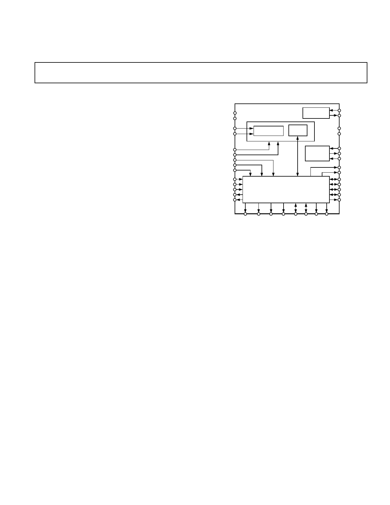
FUNCTIONAL BLOCK DIAGRAM
AVDD
AGND
VIN(+)
VIN(–)
UNI
HALF_PWR
STBY
MODE 1
MODE 2
SYNC
DVDD /CS
CFMT/ RD
DGND/ DRDY
DGND/DB0
AD7723
2.5V
REFERENCE
MODULATOR
FIR
FILTER
XTAL
CLOCK
CONTROL
LOGIC
REF2
REF1
DVDD
DGND
XTAL_OFF
XTAL
CLKIN
DGND/DB15
DGND/DB14
SCR/DB13
SLDR/DB12
SLP/DB11
TSI/DB10
FSO/DB9
DGND/ DGND/ DGND/ DOE/ SFMT/ FSI/ SCO/ SDO/
DB1 DB2 DB3 DB4 DB5 DB6 DB7 DB8
GENERAL DESCRIPTION
The AD7723 is a complete 16-bit, sigma-delta ADC. The part
operates from a +5␣ V supply. The analog input is continuously
sampled, eliminating the need for an external sample-and-hold.
The modulator output is processed by a finite impulse response
(FIR) digital filter. The on-chip filtering combined with a high
oversampling ratio reduces the external antialias requirements
to first order in most cases. The digital filter frequency response
can be programmed to be either low pass or band pass.
The AD7723 provides 16-bit performance for input bandwidths
up to 460␣ kHz at an output word rate up to 1.2 MHz. The
sample rate, filter corner frequencies and output word rate are
set by the crystal oscillator or external clock frequency.
Data can be read from the device in either serial or parallel
format. A stereo mode allows data from two devices to share a
single serial data line. All interface modes offer easy, high speed
connections to modern digital signal processors.
The part provides an on-chip 2.5␣ V reference. Alternatively, an
external reference can be used.
A power-down mode reduces the idle power consumption to
200 µW.
The AD7723 is available in a 44-lead PQFP package and is
specified over the industrial temperature range from –40°C to
+85°C.
Two input modes are provided, allowing both unipolar and
bipolar input ranges.
REV. 0
Information furnished by Analog Devices is believed to be accurate and
reliable. However, no responsibility is assumed by Analog Devices for its
use, nor for any infringements of patents or other rights of third parties
which may result from its use. No license is granted by implication or
otherwise under any patent or patent rights of Analog Devices.
One Technology Way, P.O. Box 9106, Norwood, MA 02062-9106, U.S.A.
Tel: 781/329-4700 World Wide Web Site: http://www.analog.com
Fax: 781/326-8703
© Analog Devices, Inc., 1998
1 page 
AD7723
CLKIN
2.3V
FSI
t5
0.8V
t1
t4
t6
t3
t7
t2
SCO
t8
t9
t9
t10
Figure 2. Serial Mode Timing for Clock Input, Frame Sync Input and Serial Clock Output
CLKIN
32 CLKIN CYCLES
FSI
(SFMT = 1)
SCO
(CFMT = 0)
FSO
(SFMT = 0)
FSO
(SFMT = 1)
SDO
t8
t14
t11
t12
t13
D15 D14 D13
t11
D2 D1 D0
D15 D14
Figure 3. Serial Mode 1. Timing for Frame Sync Input, Frame Sync Output, Serial Clock Output and Serial Data Output
(Refer to Table I for Control Inputs, TSI = DOE)
32 CLKIN CYCLES
CLKIN
t8
FSI
SCO
(CFMT = 0)
FSO
SDO
t14
t11
t12
t13
D2 D1 D0 D15 D14 D13 D12 D11
D5 D4 D3 D2 D1 D0 D15 D14
Figure 4. Serial Mode 2. Timing for Frame Sync Input, Frame Sync Output, Serial Clock Output and Serial Data Output
(Refer to Table I for Control Inputs, TSI = DOE)
REV. 0
–5–
5 Page 
AD7723
Mnemonic
CFMT/RD
Pin No.
4
DOE/DB4
43
SFMT/DB5
42
FSI/DB6
SCO/DB7
SDO/DB8
FSO/DB9
TSI/DB10
41
40
38
37
36
SLP/DB11
SLDR/DB12
35
34
SCR/DB13
33
DVDD/CS
DGND/DB14
DGND/DB15
DGND/DRDY
DGND/DB0
DGND/DB1
DGND/DB2
DGND/DB3
30
32
31
5
3
2
1
44
SERIAL MODE PIN FUNCTION DESCRIPTIONS
Description
Serial Clock Format Logic Input. The clock format pin selects whether the serial data, SDO, is valid
on the rising or falling edge of the serial clock, SCO. When CFMT is logic low, serial data is valid on
the falling edge of the serial clock, SCO. If CFMT is logic high, SDO is valid on the rising edge of
SCO.
Data Output Enable Logic Input. The DOE pin controls the three-state output buffer of the SDO
pin. The active state of DOE is determined by the logic level on the TSI pin. When the DOE logic
level equals the level on the TSI pin the serial data output, SDO, is active. Otherwise SDO will be
high impedance. SDO can be three-state after a serial data transmission by connecting DOE to FSO.
In normal operations, TSI and DOE should be tied low.
Serial Data Format Logic Input. The logic level on the SFMT pin selects the format of the FSO
signal for Serial Mode 1. A logic low makes the FSO output a pulse, one SCO cycle wide at the
beginning of a serial data transmission. With SFMT set to a logic high, the FSO signal is a frame
pulse that is active low for the duration of the 16-bit transmission. For Serial Modes 2 and 3, SFMT
should be tied high.
Frame Synchronization Logic Input. The FSI input is used to synchronize the AD7723 serial output
data register to an external source and to allow more than one AD7723, operated from a common
master clock, to simultaneously sample its analog input and update its output register.
Serial Clock Output.
Serial Data Output. The serial data is shifted out MSB first, synchronous with the SCO. Serial
Mode 1 data transmissions last 32 SCO cycles. After the LSB is output, trailing zeros are output for
the remaining 16 SCO cycles. Serial Modes 2 and 3 data transmissions last 16 SCO cycles.
Frame Sync Output. FSO indicates the beginning of a word transmission on the SDO pin. Depend-
ing on the logic level of the SFMT pin, the FSO signal is either a positive pulse approximately one
SCO period wide, or a frame pulse which is active low for the duration of the 16-data bit transmission.
Time Slot Logic Input. The logic level on TSI sets the active state of the DOE pin. With TSI set
logic high, DOE will enable the SDO output buffer when it is a logic high, and vice versa. TSI is
used when two AD7723s are connected to the same serial data bus. When this function is not
needed, TSI and DOE should be tied low.
Serial Mode Low Pass/Band Pass Filter Select Input. With SLP set logic high, the low-pass filter
response is selected. A logic low selects band pass.
Serial Mode Low/High Output Data Rate Select Input. With SLDR set logic high, the low data rate
is selected. A logic low selects the high data rate. The high data rate corresponds to data at the out-
put of the fourth decimation filter (Decimate by 16). The low data rate corresponds to data at the
output of the fifth decimation filter (Decimate by 32).
Serial Clock Rate Select Input. With SCR set logic low, the serial clock output frequency, SCO, is
equal to the CLKIN frequency. A logic high sets it equal to one-half the CLKIN frequency.
Tie to DVDD.
Tie to DGND.
Tie to DGND.
Tie to DGND.
Tie to DGND.
Tie to DGND.
Tie to DGND.
Tie to DGND.
REV. 0
–11–
11 Page | ||
| Páginas | Total 23 Páginas | |
| PDF Descargar | [ Datasheet AD7723.PDF ] | |
Hoja de datos destacado
| Número de pieza | Descripción | Fabricantes |
| AD7720 | CMOS Sigma-Delta Modulator | Analog Devices |
| AD7721 | CMOS 16-Bit/ 468.75 kHz/ Sigma-Delta ADC | Analog Devices |
| AD7722 | 16-Bit/ 195 kSPS CMOS/ Sigma-Delta ADC | Analog Devices |
| AD7723 | 16-Bit/ 1.2 MSPS CMOS/ Sigma-Delta ADC | Analog Devices |
| Número de pieza | Descripción | Fabricantes |
| SLA6805M | High Voltage 3 phase Motor Driver IC. |
Sanken |
| SDC1742 | 12- and 14-Bit Hybrid Synchro / Resolver-to-Digital Converters. |
Analog Devices |
|
DataSheet.es es una pagina web que funciona como un repositorio de manuales o hoja de datos de muchos de los productos más populares, |
| DataSheet.es | 2020 | Privacy Policy | Contacto | Buscar |